Etching method for stacked metal gate

A metal gate and stacking technology, which is applied in the field of etching of stacked metal gates, can solve problems such as affecting device stability, and achieve the effect of improving stability and avoiding over-etching.

Active Publication Date: 2012-01-11
SHANGHAI HUAHONG GRACE SEMICON MFG CORP
View PDF6 Cites 11 Cited by
  • Summary
  • Abstract
  • Description
  • Claims
  • Application Information

AI Technical Summary

Problems solved by technology

[0009] In the process of forming a stacked metal gate using the existing etching technology, after the warm-up etching is performed on the control chip, the first product wafer in a batch of product wafers is subjected to main etching to form a stacked metal gate At this time, the line width (CD) of the stacked metal gate is 6-9 nanometers smaller than the line width of the stacked metal gate formed on the other product wafers of the same batch. The small line width effect of the metal gate greatly affects the stability of the device

Method used


Image

  • Etching method for stacked metal gate
  • Etching method for stacked metal gate
  • Etching method for stacked metal gate

Examples


Embodiment Construction

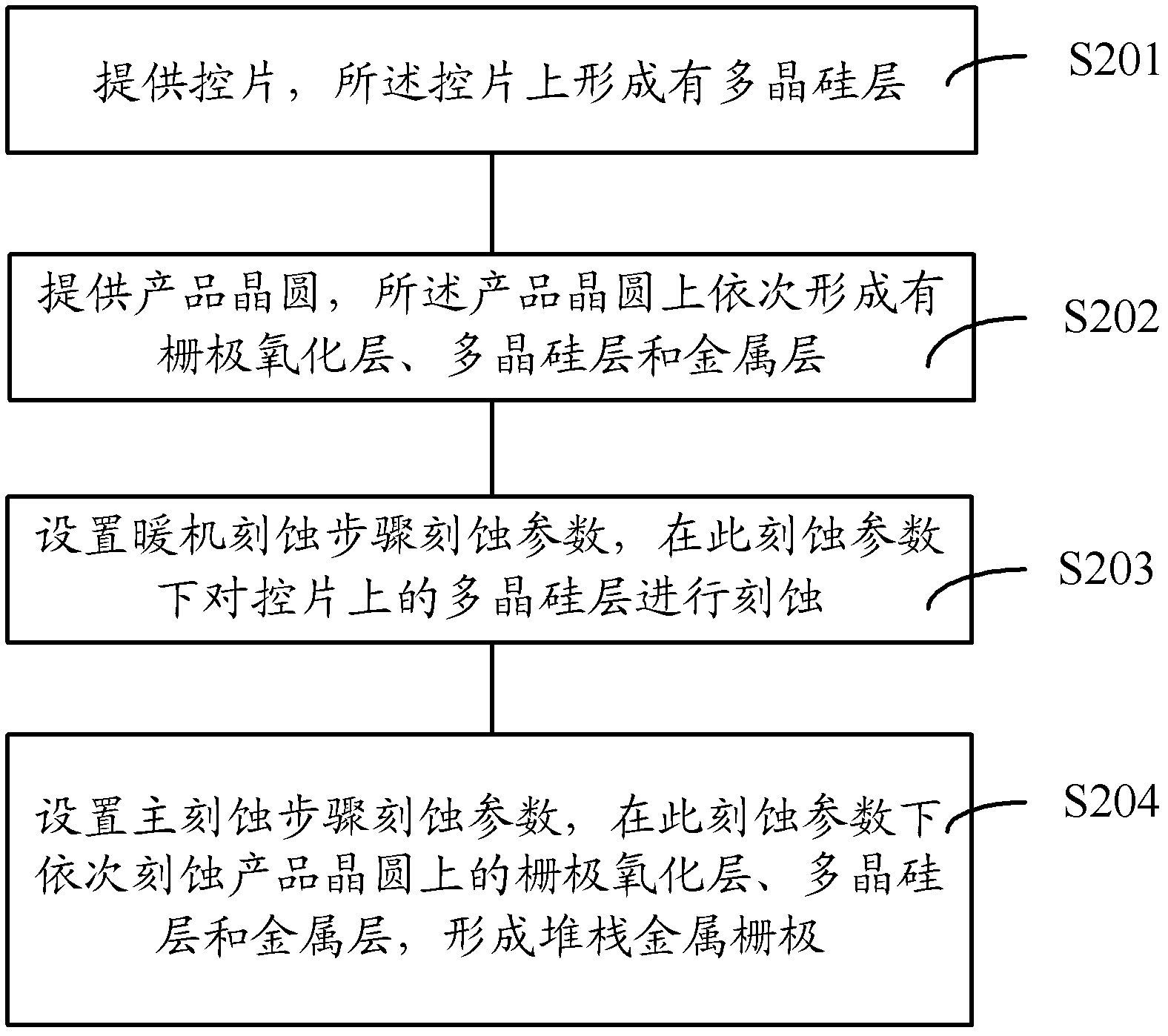
[0032] In the process of etching the stacked tungsten metal gate using the prior art, the inventor found that during the warm-up etching step, if the same stack as the metal gate is formed on the control chip used, after the warm-up etching process, the main etching The etching process can basically eliminate the small line width effect of the stacked metal gate formed on the first product wafer, but the same stacking as the tungsten metal gate is formed on the control wafer, which increases the manufacturing cost.

[0033] The inventors have further studied and found that the warm-up etching step and the main etching step adopt the same etching menu, and the gas used in the main etching step is nitrogen trifluoride (NF 3 ), Chlorine (Cl 2 ) and hydrogen bromide (HBr), the warm-up etch step also uses nitrogen trifluoride (NF 3 ), Chlorine (Cl 2 ) and hydrogen bromide (HBr), the plasma (fluorine ion and chlorine ion) that chlorine gas, nitrogen trifluoride produces is used fo...


PUM


Abstract

The invention relates to an etching method for a stacked metal gate. The method comprises the following steps that: a control wafer is provided and a polysilicon layer is formed on the control wafer; a product wafer is provided, wherein a gate oxide, a polysilicon layer and a metal layer are successively formed on the product wafer; an etching parameter of a season etching step is arranged and the polysilicon layer on the control wafer is etched on the basis of the etching parameter; an etching parameter of a main etching step is arranged and the gate oxide, the polysilicon layer and the metal layer on the product wafer are successively etched on the basis of the etching parameter, so that a stacked metal gate is formed. On the basis of the utilization of the etching method provided in the invention, an effect of small linewidth of a stacked metal gate of a first piece of product wafer after the season etching can be eliminated, so that stability of a device is improved.

Description

technical field [0001] The invention relates to the field of semiconductor manufacturing, in particular to an etching method for stacked metal gates. Background technique [0002] In the semiconductor integrated circuit manufacturing process, a semiconductor structure is formed on a semiconductor substrate through a series of deposition, photolithography, etching, and planarization processes. Among them, the photolithography process is to form a mask pattern and define the area to be etched; and the etching process is used to transfer the pattern defined by the photolithography into the material layer. As the manufacturing process of large-scale integrated circuits advances to submicron and deep submicron, the requirements for the accuracy and repeatability of the etching process are getting higher and higher. The existing method to maintain the stability of the etching chamber conditions is to perform a warm-up (Season) etching in the etching chamber before product etching...

Claims


Application Information

Patent Timeline
Patent Type & Authority Applications(China)
IPC IPC(8): H01L21/28H01L21/3213
Inventor 熊磊奚裴
Owner SHANGHAI HUAHONG GRACE SEMICON MFG CORP
Why Eureka
Try Eureka