Super-junction semiconductor device with groove-type terminal structure

A terminal structure and semiconductor technology, which is applied in the direction of semiconductor devices, electrical components, circuits, etc., can solve problems such as forming methods, achieve the effects of reducing grinding time, reducing production costs, and improving filling efficiency

Active Publication Date: 2012-01-11
SHANGHAI HUAHONG GRACE SEMICON MFG CORP
View PDF3 Cites 11 Cited by
  • Summary
  • Abstract
  • Description
  • Claims
  • Application Information

AI Technical Summary

Problems solved by technology

[0003] Although super-junction MOSFETs can provide lower on-resistance while maintaining a higher breakdown voltage, there are still many p

Method used


Image

  • Super-junction semiconductor device with groove-type terminal structure
  • Super-junction semiconductor device with groove-type terminal structure
  • Super-junction semiconductor device with groove-type terminal structure

Examples


Embodiment 1

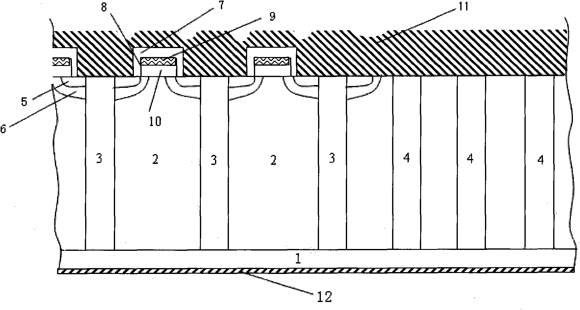
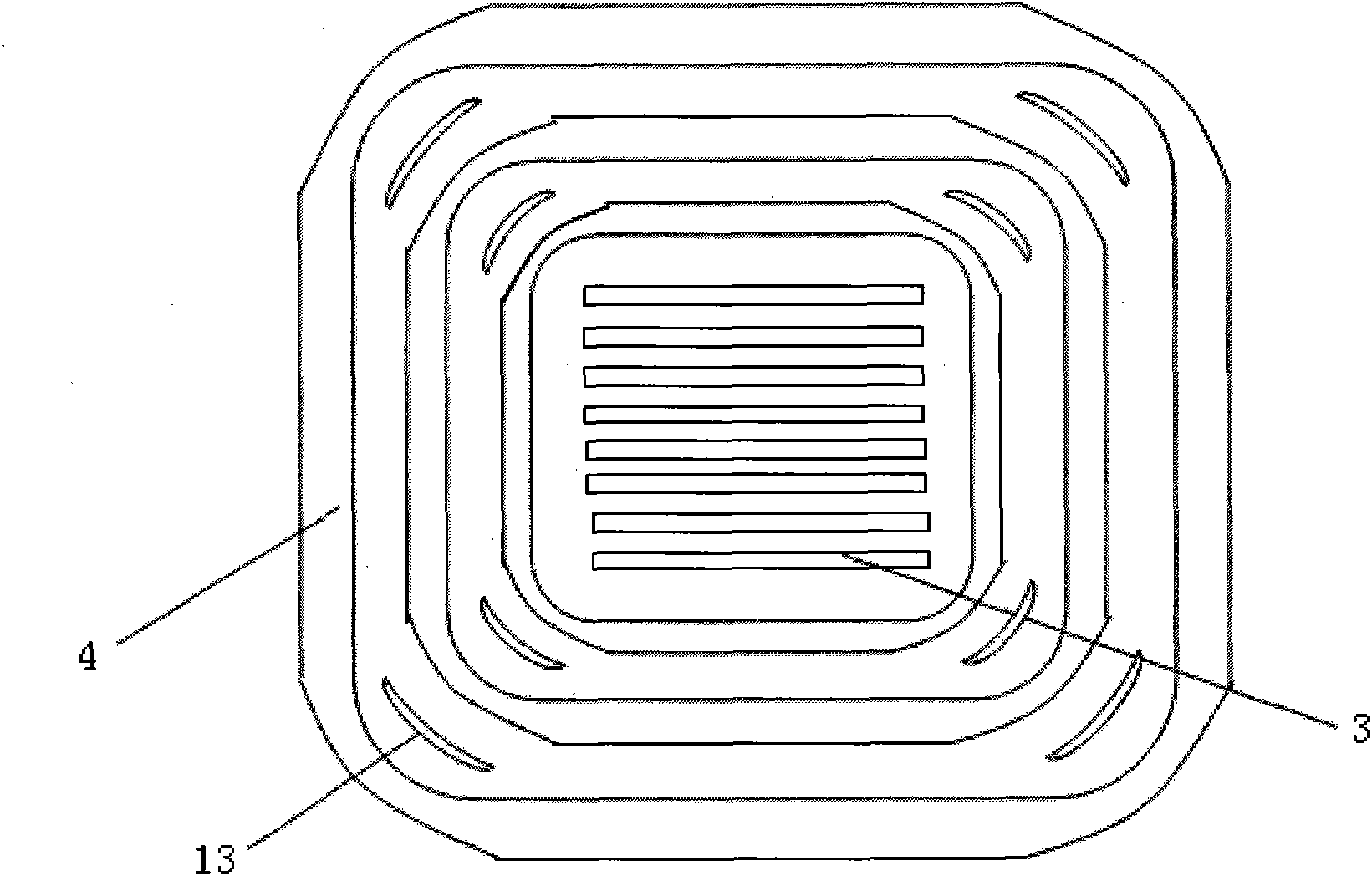
[0040] combine figure 1As shown, an N-type epitaxial layer (semiconductor region 2 ), such as a P-doped low-doped epitaxial layer with a thickness of 50 μm, is grown on a heavily doped silicon substrate (semiconductor substrate 1 ). Subsequently, a source region 5 and a base region 6 are formed on the N-type epitaxial layer. Growth of a deep trench etch stop (hard mask) or a CMP polish stop such as an oxide, nitride or oxynitride layer. The barrier layer can be a single layer or multilayer, such as first oxide+second oxide, or oxide+nitride, or oxide+nitride+oxide. Then define a deep trench etching area, that is, the first trench 3, the second trench 4, and the third trench 13, and perform deep trench etching. The crystal plane of the main sidewall of the trench is (100). For example, the width of the first trench 3 is 5 μm, the width of the second trench 4 is 5 μm at the straight side, the width at the corner is 4 μm, and the width of the second trench 4 is 1 μm. All three...

Embodiment 2

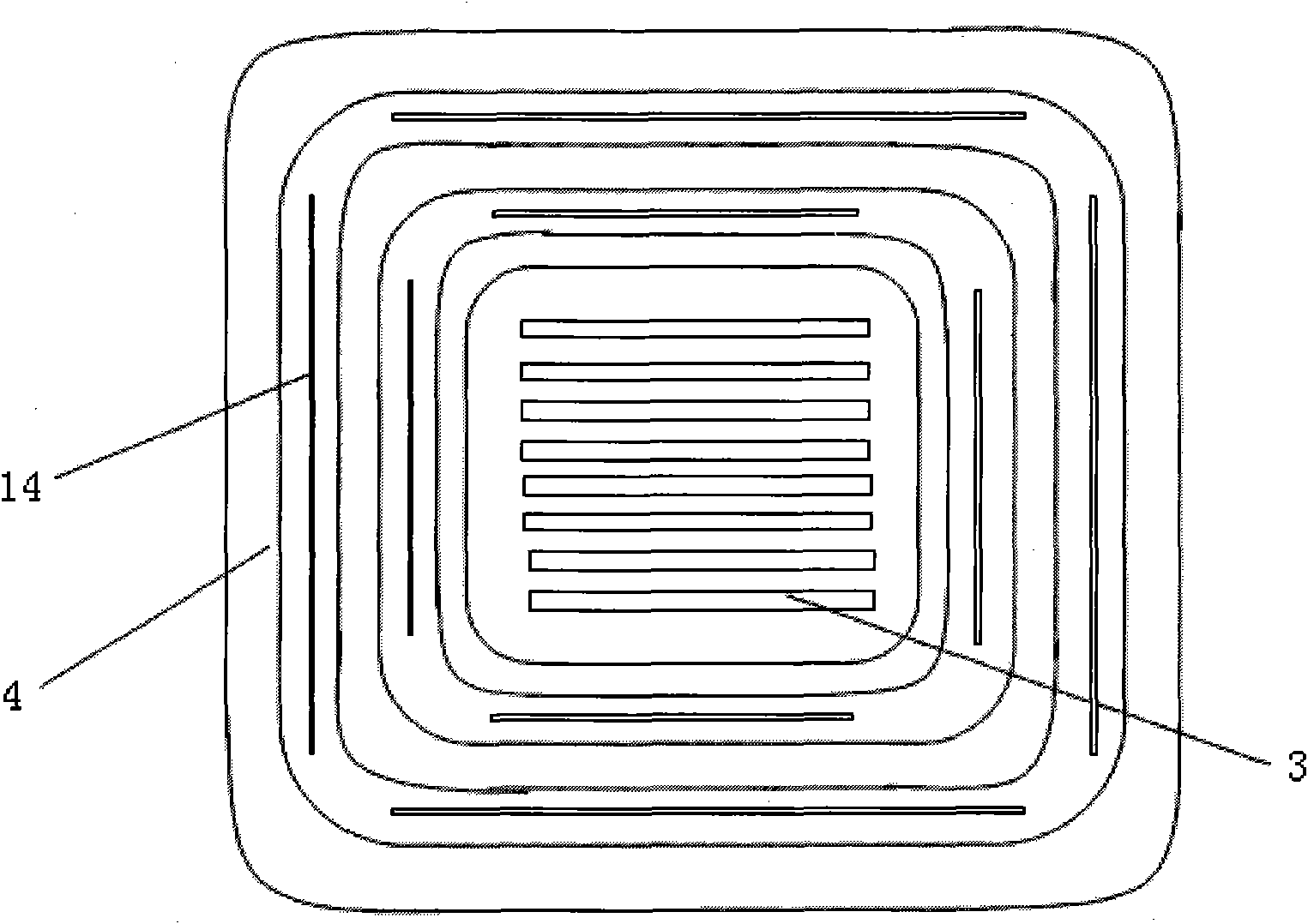
[0042] combine figure 1 As shown, an N-type epitaxial layer (semiconductor region 2 ), such as a P-doped low-doped epitaxial layer with a thickness of 50 μm, is grown on a heavily doped silicon substrate (semiconductor substrate 1 ). Subsequently, a source region 5 and a base region 6 are formed on the N-type epitaxial layer. A deep trench etch stop (hard mask) or CMP polish stop is then grown; such as oxide, nitride or oxynitride. The barrier layer can be a single layer or multilayer, such as first oxide+second oxide, or oxide+nitride, or oxide+nitride+oxide. Then define a deep trench etching area, that is, the area of ​​the first trench 3 , the second trench 4 and the fourth trench 14 , and perform deep trench etching. The crystal plane of the main sidewall of the trench is (110). For example, the width of the first trench 3 is 4 μm, the width of the second trench 4 is 4 μm at the straight side, the width at the corner is 5 μm, and the width of the fourth trench 14 is 1 μm...


PUM

PropertyMeasurementUnit
Thicknessaaaaaaaaaa

Abstract

The invention discloses a super-junction semiconductor device with a groove-type terminal structure. The super-junction semiconductor device comprises a semiconductor substrate, a first electrode, a semiconductor region, an active device, a base region, a source region, an insulation control electrode, a passivation insulating layer, a plurality of second grooves and a second electrode, wherein the semiconductor region comprises an active region and a terminal region; the active device is formed in the active region and comprises a plurality of first grooves arranged at equal intervals; the plurality of second grooves are formed in the terminal region; a semiconductor material with a second conductive type is filled in the first grooves and the second grooves; the second electrode is continuously coated on the passivation insulating layer and the second grooves; the surfaces of the second grooves are in a ring shape and encircle the active region, the corners of the annular second grooves are in an arc shape, and the other parts are in a straight line shape; and the width of the corners is not equal to that of straight line. By the super junction semiconductor device, a super-junction terminal structure can be optimized, and the epitaxial growth cost is reduced.

Description

technical field [0001] The invention relates to the field of semiconductor integrated circuits, in particular to a super junction semiconductor device with a trench terminal structure. Background technique [0002] The super-junction MOSFET adopts a structure of alternately arranged N-type and P-type column layers (that is, semiconductor thin layers). For an N-channel MOSFET, in the on state, the conduction current flows through the N-type column; in the off state, the P-type region and the N-type region deplete each other to obtain a high breakdown voltage. Since a thinner N-type epitaxial layer and a higher N-type doping amount can be used without worrying about the reduction of the breakdown voltage, a lower on-resistance (Rson) can be obtained while maintaining a high breakdown voltage. For P-channel MOSFETs, do the opposite. [0003] Although super-junction MOSFETs can provide lower on-resistance while maintaining a higher breakdown voltage, there are still many probl...

Claims


Application Information

Patent Timeline
IPC IPC(8): H01L29/06H01L29/78
Inventor 刘继全谢烜
Owner SHANGHAI HUAHONG GRACE SEMICON MFG CORP
Why Eureka
Try Eureka