
Circuit board and manufacturing method thereof

A circuit board production and circuit board technology, which is applied in the direction of printed circuit components, electrical connection printed components, and printed component electrical connection formation, can solve the problem of double-sided circuit boards that are difficult to meet the requirements of light weight and miniaturization of portable electronic devices. Problems such as large thickness and weight

Active Publication Date: 2012-01-11
HONGQISHENG PRECISION ELECTRONICS (QINHUANGDAO) CO LTD +1
View PDF3 Cites 9 Cited by
  • Summary
  • Abstract
  • Description
  • Claims
  • Application Information

AI Technical Summary

Problems solved by technology

However, due to the large thickness and weight of double-sided circuit boards or multi-layer circuit boards, it is difficult to meet the requirements of light weight and miniaturization of portable electronic devices

Method used


Image

  • Circuit board and manufacturing method thereof
  • Circuit board and manufacturing method thereof
  • Circuit board and manufacturing method thereof

Examples


Embodiment Construction

[0049] The circuit board provided by the technical solution and its manufacturing method will be further described in detail below in conjunction with the accompanying drawings and embodiments.

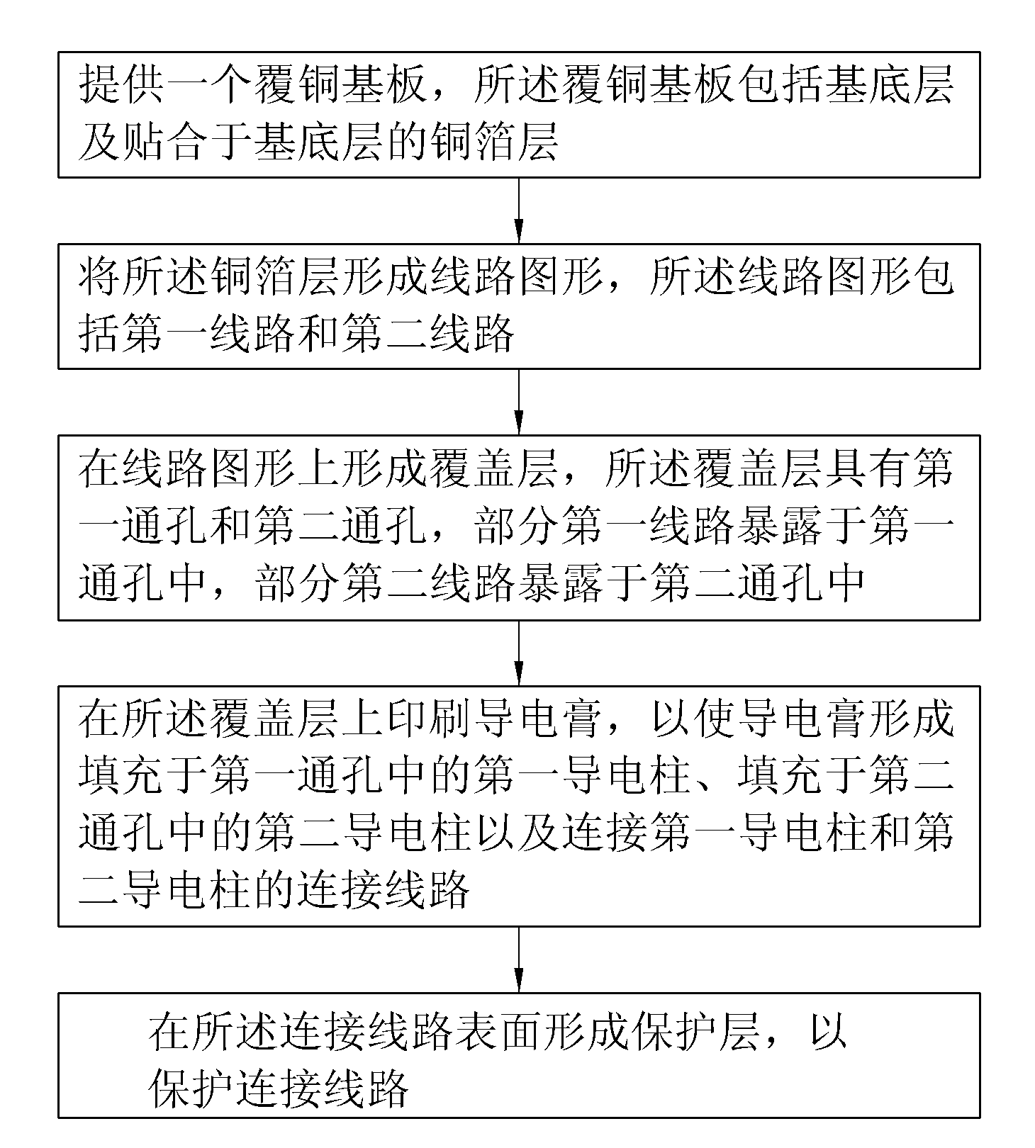
[0050] see figure 1 The circuit board manufacturing method provided by the embodiment of the technical solution includes the steps:

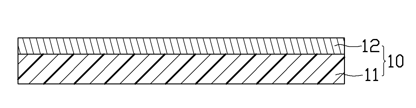
[0051] For a first step, see figure 2 , providing a copper-clad substrate 10 , the copper-clad substrate 10 includes a base layer 11 and a copper foil layer 12 attached to the base layer 11 .

[0052]In this embodiment, the copper clad substrate 10 is a single-layer copper foil substrate, that is, it only includes one copper foil layer 12 . The material of the base layer 11 can be a hard material, such as epoxy resin, glass fiber cloth, etc., or a flexible material, such as polyimide (Polyimide, PI), polyethylene terephthalate ( Polyethylene Terephthalate (PET), Teflon, Polyamide, Polymethylmethacrylate, Polycarbonate or Polyimide-Polyethylene-Terep...


PUM


Abstract

The invention provides a method for manufacturing a circuit board, and the method comprises the following steps: providing a copper-clad substrate, wherein the copper-clad substrate comprises a base layer and a copper foil layer; enabling the copper foil layer to be formed into a circuit diagram, wherein the circuit diagram comprises a first circuit and a second circuit; forming a covering layer on the circuit diagram, wherein the covering layer is provided with a first through hole and a second through hole, part of the first circuit is exposed to the first through hole, and part of the second circuit is exposed to the second through hole; printing a conductive paste on the covering layer, so that the conductive paste is formed into a first conductive column filled in the first through hole, a second conductive column filled in the second through hole and a first connecting circuit connecting the first conductive column with the second conductive column, thus the first circuit is electrically connected with the second circuit through the first conductive column, the first connecting circuit and the second conductive column; and forming a protective layer on the surface of the first connecting circuit. The invention also provides a circuit board manufactured by using the method for manufacturing the circuit board, and the circuit board is relatively light and thin.

Description

technical field [0001] The invention relates to the technical field of circuit boards, in particular to a light and thin circuit board and a manufacturing method thereof. Background technique [0002] In the information, communication and consumer electronics industries, circuit boards are an indispensable and basic component of all electronic information products. However, in portable electronic devices that require lightness, thinness, shortness, and smallness, such as mobile phones, it is necessary to use relatively thin and light circuit boards to realize circuit connections in a small space. With the improvement of people's requirements for portable electronic devices to process information, the lines on the circuit board are becoming more and more dense, and it is necessary for the lines to cross the cross-connect to realize the transmission and processing of electrical information. At this time, it is usually necessary to make the circuit board into a double-sided ci...

Claims


Application Information

Patent Timeline
IPC IPC(8): H05K3/40H05K3/42H05K1/11
Inventor 郑建邦
Owner HONGQISHENG PRECISION ELECTRONICS (QINHUANGDAO) CO LTD
Features
  • Generate Ideas
  • Intellectual Property
  • Life Sciences
  • Materials
  • Tech Scout
  • Unparalleled Data Quality
  • Higher Quality Content
  • 60% Fewer Hallucinations
Learn More