Optimization method of optical proximity effect correction based on Abbe vector imaging model

A technology of optical proximity effect and imaging model, applied in optics, originals for photomechanical processing, micro-lithography exposure equipment, etc., can solve the problem of inapplicable lithography system, difference in function of projection system, influence on mask optimization effect, etc. problem, to achieve the effect of high precision and high optimization efficiency

Inactive Publication Date: 2012-01-18
BEIJING INSTITUTE OF TECHNOLOGYGY
View PDF7 Cites 10 Cited by
  • Summary
  • Abstract
  • Description
  • Claims
  • Application Information

AI Technical Summary

Problems solved by technology

However, the above method is based on the scalar imaging model of the lithography system, so it is not suitable for high NA lithography systems
At the same time, the existing technology does not consider the difference in response of the projection system to the incident light from different point light sources on the light source surface.
Ho

Method used


Image

  • Optimization method of optical proximity effect correction based on Abbe vector imaging model
  • Optimization method of optical proximity effect correction based on Abbe vector imaging model
  • Optimization method of optical proximity effect correction based on Abbe vector imaging model

Examples


Embodiment

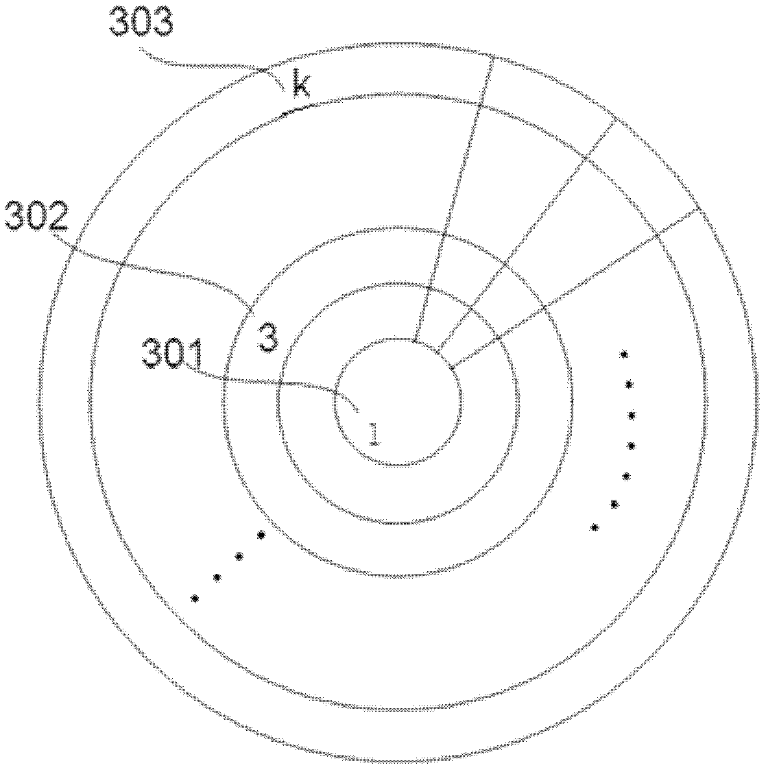
[0141] Such as Figure 4 As shown, 401 is a schematic diagram of the initial binary mask, its critical dimension is 45nm, white represents the light-transmitting region, and its reflectivity is 1, and black represents the light-blocking region, its reflectance is 0. The mask pattern is located on the XY plane, and the lines are parallel to the Y axis. 402 is the in-air imaging result of the binary mask under ring illumination obtained after rasterizing the light source surface into 31×31 point light sources. 403 is the in-air imaging result of the binary mask under ring illumination obtained after rasterizing the light source surface into 2×2 point light sources. 404 is the comparison of light intensity distribution curves at Y=0 obtained by the two methods. 405 is a light intensity distribution curve obtained after rasterizing the light source surface into 31×31 point light sources. 406 is a light intensity distribution curve obtained after rasterizing the light source int...


PUM


Abstract

The invention provides an optimization method of optical proximity effect correction based on an Abbe vector imaging model; according to the method, the transmittance of an opening part and a light-masking part of a mask is set; a variable matrix omega is set; an object function D is constructed to be the square of an euler distance between a target pattern and an image in a photoresist corresponding to the current mask; the optimization of the mask pattern is guided by the variable matrix omega and the object function D. The mask optimized by the invention is not only applicable to cases with a less NA, but also applicable to cases with a NA higher than 0.6. Meanwhile, by using gradient information of the optimized object function, and combining a steepest descent method, the invention optimizes the mask pattern with high optimization efficiency.

Description

technical field [0001] The invention relates to an optimization method for optical proximity effect correction based on an Abbe (Abbe) vector imaging model, and belongs to the technical field of lithographic resolution enhancement. Background technique [0002] The current large-scale integrated circuits are generally manufactured using photolithography systems. The lithography system is mainly divided into four parts: illumination system (including light source and condenser), mask, projection system and wafer. The light emitted by the light source is focused by the condenser and then enters the mask, and the opening part of the mask transmits light; after passing through the mask, the light is incident on the wafer coated with photoresist through the projection system, so that the pattern of the mask is copied on the wafer. [0003] The current mainstream lithography system is the 193nm ArF deep ultraviolet lithography system. As the lithography technology node enters 45n...

Claims


Application Information

Patent Timeline
IPC IPC(8): G03F7/20G03F1/36
Inventor 马旭李艳秋董立松
Owner BEIJING INSTITUTE OF TECHNOLOGYGY
Why Eureka
Try Eureka