

Preparation process for anti-oxidation copper-based bonding wires
A preparation process and bonding wire technology, applied in semiconductor/solid-state device manufacturing, electrical components, circuits, etc., can solve the problems of bonding wire packaging, high bonding wire hardness, etc. Destruction, reduction of bonding energy, effect of high bonding performance
- Summary
- Abstract
- Description
- Claims
- Application Information
AI Technical Summary
Problems solved by technology
Method used
Image

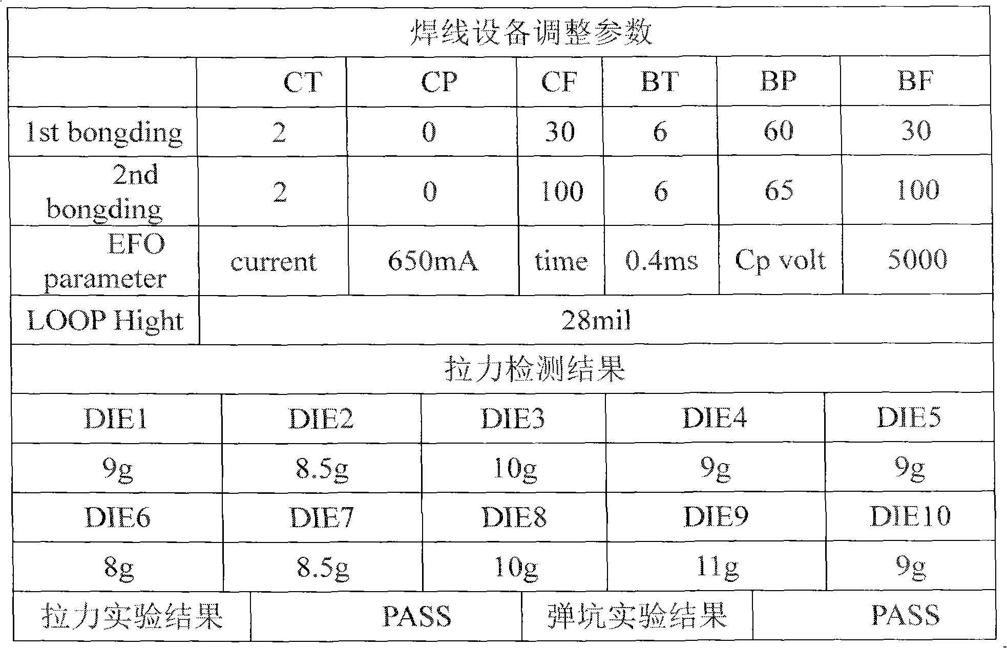
Examples
Embodiment 1
[0028] A copper-based bonding wire, the basic material is copper, and trace metal elements such as Pt, Ce, and Pd are added to form a master alloy base material, and the surface of the metal wire made of the master alloy base material is plated with a layer of gold. Among them, the purity of copper and gold plating is higher than 99.99%.
[0029] The mass proportion of each metal component in the bonding wire material is respectively: Cu is 94.9933%, trace metal element Pt is 0.0007%, Ce is 0.002%, Pd is 0.004%, gold plating is 5%, and the diameter of the bonding wire is 50 microns , the thickness of the gold layer is 0.6 microns.
[0030] The preparation of copper-based bonding wire comprises the following steps:
[0031] Step one, mixing metal substrates. Cu with a purity higher than 99.99%, plus selected trace metal materials Pt, Ce, and Pd, is mixed as a master alloy base material, and the preliminary preparation for mixing and smelting is done.
[0032] Step 2, melting...
Embodiment 2
[0040]A copper-based bonding wire, the basic material is copper, and trace metal elements such as Pt, Ce, and Pd are added to form a master alloy base material, and the surface of the metal wire made of the master alloy base material is plated with a layer of gold. Among them, the purity of copper and gold plating is higher than 99.99%.
[0041] The mass proportion of each metal component in the bonding wire material is respectively: Cu is 95.9923%, the trace metal element Pt is 0.0007%, Ce is 0.004%, Pd is 0.003%, gold-plated gold is 4%, and the diameter of the bonding wire is 50 Micron, the thickness of the gold layer is 0.5 micron.
[0042] The preparation technology of described copper-based bonding wire comprises the following steps:
[0043] Step one, mixing metal substrates. Cu with a purity higher than 99.99%, plus selected trace metal materials Pt, Ce, and Pd, is mixed as a master alloy base material, and the preliminary preparation for mixing and smelting is done. ...
PUM
| Property | Measurement | Unit |
|---|---|---|
| thickness | aaaaa | aaaaa |
| diameter | aaaaa | aaaaa |
Abstract
Description
Claims
Application Information