High-power semiconductor laser light source system for laser processing

A laser light source and laser processing technology, applied in semiconductor laser devices, laser devices, laser welding equipment, etc., can solve the problems of low photoelectric conversion rate, short life, high cost, and achieve low system cost, long life, and large working distance. Effect

Inactive Publication Date: 2012-01-18
FOCUSLIGHT TECH
View PDF6 Cites 8 Cited by
  • Summary
  • Abstract
  • Description
  • Claims
  • Application Information

AI Technical Summary

Problems solved by technology

[0008] The main purpose of the present invention is to overcome the shortcomings of the above-mentioned prior art, provide a high-power semiconductor laser light source system for laser processing, and solve the problems of low photoelectric conversion rate, large volume, high cost, and short life in current laser processing systems. question

Method used


Image

  • High-power semiconductor laser light source system for laser processing
  • High-power semiconductor laser light source system for laser processing
  • High-power semiconductor laser light source system for laser processing

Examples


Embodiment 1

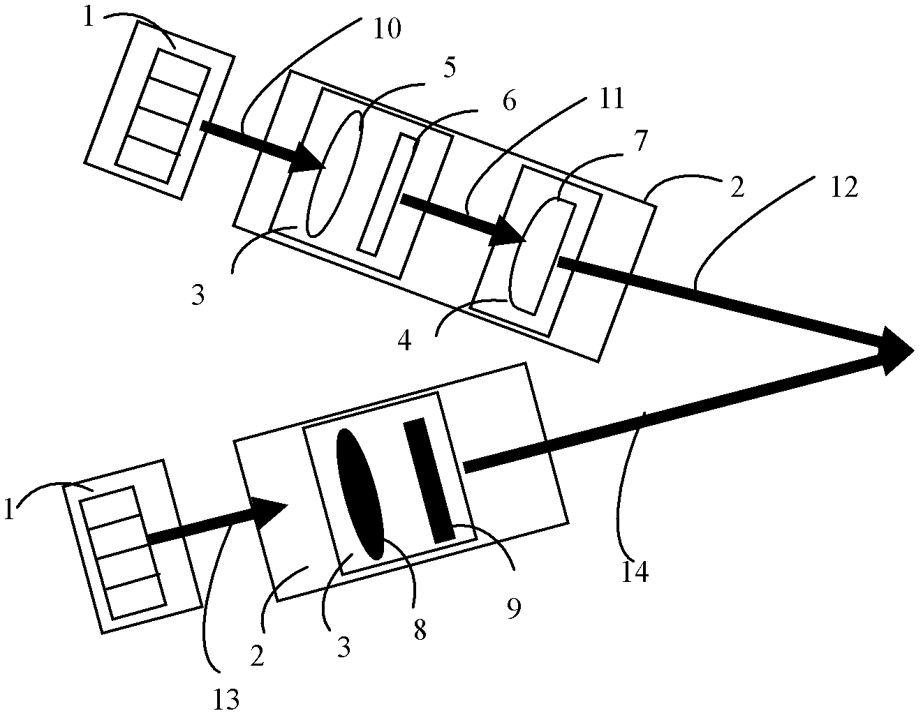
[0034] Such as figure 1 As shown, the basic structure adopted in this embodiment is the same as the structure explained above, including two semiconductor laser stacks 1 and shaping lens groups 2, and the two semiconductor laser stacks 1 and the shaping lens groups 2 at the rear end form an angle α is placed and arranged in a fan shape so that the shaped beams are superimposed and output.

[0035] For the first semiconductor laser stack 1, it is composed of 40 bar chips with microlenses. After the semiconductor laser stack 1, a shaping lens group 2 is set. The shaping lens group 2 includes a fast axis shaping lens group 3 and Slow axis shaping lens group 4 , fast axis shaping lens group 3 includes two spherical lenses 5 and 6 , slow axis shaping lens group 4 includes aspheric lens 7 .

[0036] For the second semiconductor laser stack 1, it is composed of 40 bar chips with microlenses. After the semiconductor laser stack 1, a shaping lens group 2 is arranged. The shaping lens ...

Embodiment 2

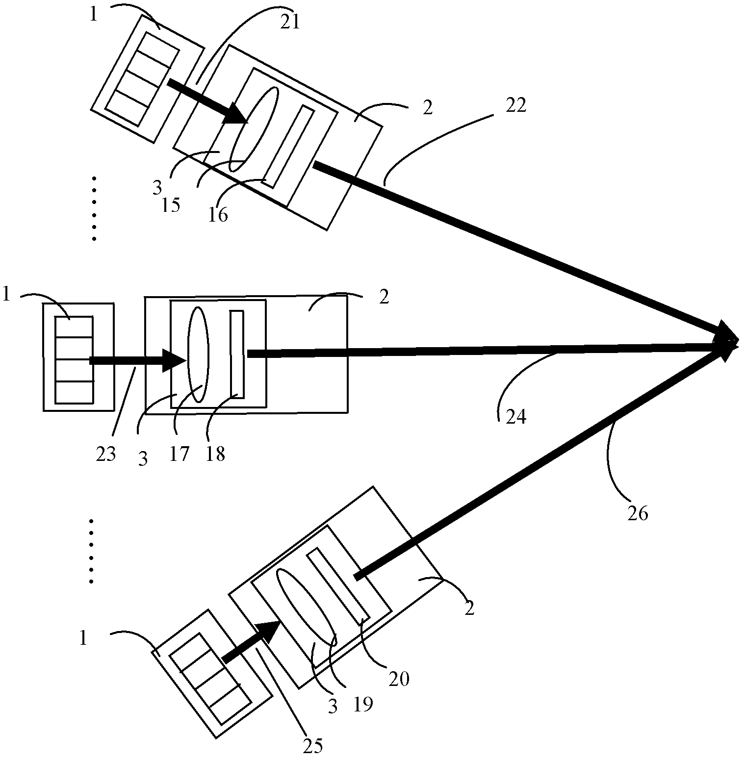
[0039] Such as image 3 As shown, it includes four semiconductor laser stacks 1 and a shaping lens group 2, and the four semiconductor laser stacks 1 are arranged in a fan shape, a cone shape, or a hemispherical shape.

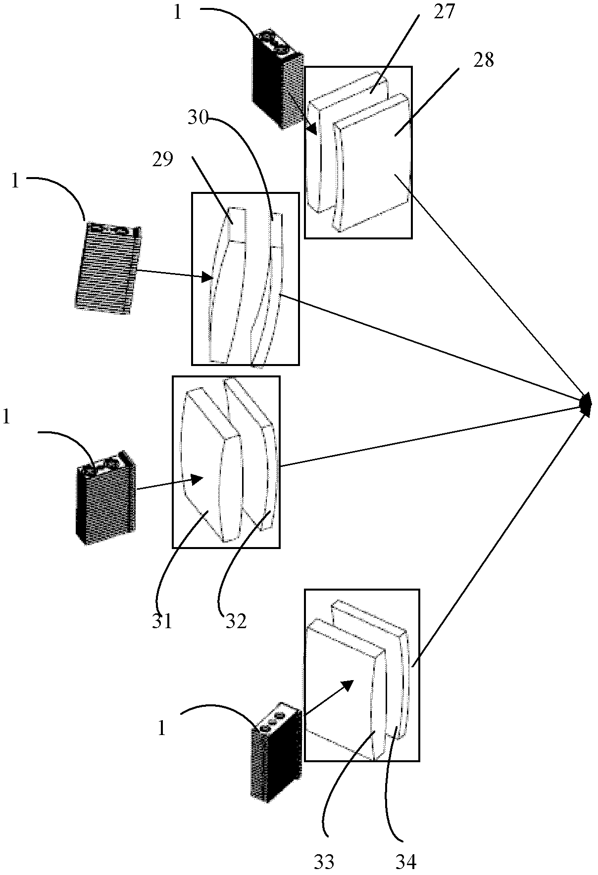
[0040] For the first semiconductor laser stack 1, it is composed of 50 bar chips with micro-lenses added. After the semiconductor laser stack 1, a shaping lens group 2 is set. The shaping lens group 2 includes two fast-axis collimating spherical surfaces. Lenses 27 and 28.

[0041] For the second semiconductor laser stack 1, it consists of 50 bar chips with micro-lenses superimposed. After the semiconductor laser stack 1, a shaping lens group 2 is set. The shaping lens group 2 includes two fast-axis collimating spherical lenses. 29 and 30.

[0042] For the third semiconductor laser stack 1, it is composed of 50 bar chips with micro-lenses added. After the semiconductor laser stack 1, a shaping lens group 2 is set, and the shaping lens group 2 has two fast-ax...


PUM


Abstract

The invention discloses a high-power semiconductor laser light source system for laser processing. The high-power semiconductor laser light source system for laser processing comprises a plurality of semiconductor laser stack arrays and shaping lens groups, wherein the semiconductor laser stack arrays are arranged in a sector shape or a cone shape or a spherical shape as a whole; the shaping lens groups are individually arranged in a manner of respectively corresponding to each semiconductor laser stack array; and optical axes formed by various semiconductor laser stack arrays and corresponding shaping lens groups are converged at the outlet of the high-power semiconductor laser light source system. The high-power semiconductor laser light source system for laser processing, disclosed by the invention, has the advantages of simple principle, small volume, high electro-optic conversion efficiency, high power, high brightness, adjustable power, capability of realizing myriawatt-level output and capability of being directly applied to the field of laser processing.

Description

technical field [0001] The invention belongs to the technical field of laser processing, and relates to a semiconductor laser light source system, in particular to a high-power semiconductor laser light source system for laser processing. Background technique [0002] Due to the advantages of small size, light weight, high efficiency and long life, high-power semiconductor lasers have been widely used in laser processing, laser medical treatment, laser display and scientific research. , Comprehensive high-tech with a wide range of applications. [0003] Laser processing technology is a high-tech fusion of modern physics, chemistry, computer, material science, advanced manufacturing technology and other multidisciplinary technologies, including laser surface modification technology, laser surface repair technology, laser cladding technology, laser productization technology, etc. , enabling low-grade materials to achieve high-performance surface modification, achieving the be...

Claims


Application Information

Patent Timeline
Patent Type & Authority Applications(China)
IPC IPC(8): H01S5/40B23K26/06B23K26/064
Inventor 刘兴胜王敏郑艳芳王晓飚
Owner FOCUSLIGHT TECH
Why Eureka
Try Eureka