

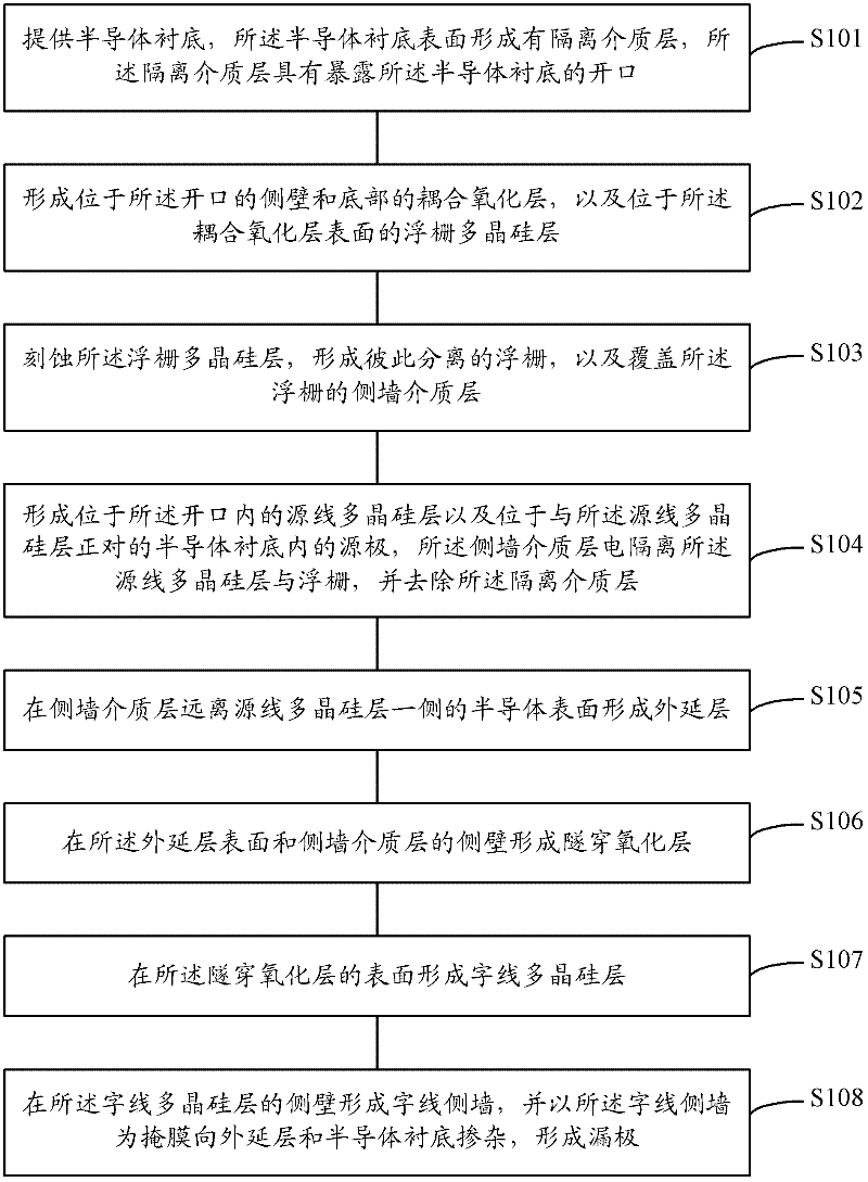
Split-gate flash memory unit and forming method thereof
A flash memory cell and split gate technology, which is applied in the manufacturing of electrical components, electric solid state devices, semiconductor/solid state devices, etc., can solve the problem of insufficient efficiency of split gate flash memory cells, reduce programming interference, increase the number, and is conducive to small the effect of
- Summary
- Abstract
- Description
- Claims
- Application Information
AI Technical Summary
Problems solved by technology
Method used
Image

Examples
Embodiment Construction
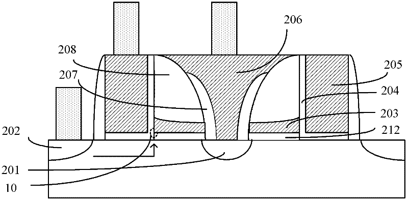
[0045] It can be seen from the background art that the programming efficiency of the existing split-gate flash memory cells is not high enough. refer to figure 1 When programming the existing split-gate flash memory unit, a high potential is applied to the polysilicon layer 206 of the source line. In the semiconductor substrate facing the polysilicon layer 206; at the same time, the high potential will be coupled to the floating gate 203, and the floating gate 203 will generate a coupling voltage. Under the action of the coupling voltage, electrons will go along figure 1 The path indicated by the middle arrow is implanted into the floating gate 203 from the region of the floating gate 203 close to the drain 202 , so as to realize programming.
[0046] After research, the inventor found that because the channel region between the source 201 and the drain 202 has a relatively large height difference from the floating gate 203, electrons need to be deflected at a relatively larg...
PUM
 Abstract
Description
Claims
Application Information