Substrate temperature control method

A technology for controlling substrates and substrates, used in semiconductor/solid-state device manufacturing, ion implantation plating, gaseous chemical plating, etc., can solve problems such as temperature rise, clean room safety risks, leakage, adhesion pollution, etc. Effect

Inactive Publication Date: 2012-02-15
CANON ANELVA CORP
View PDF8 Cites 8 Cited by
  • Summary
  • Abstract
  • Description
  • Claims
  • Application Information

AI Technical Summary

Problems solved by technology

With this control method, the above-mentioned heat input can be controlled in a steady state, but in an environment where heat input such as plasma is generated transiently, since the thermal conductivity of the heat transfer member is as small as 0.3 to 1W / K, the temperature of the substrate Temporary rise to nearly 2 times the set temperature
In addition, it takes more than 10 seconds until the temperature is stably controlled to the set temperature.
[0017] In addition, in this temperature control method, there is the following problem: the desired process performance cannot be obtained due to the change of the substrate temperature during the process
Since the circulating medium of this kind of substrate holding device is oily, it is easy to cause pollution due to leakage and adhesion during maintenance, which is not conducive to the operation in the clean room
The cooling medium (circulating medium) is often a material with ignitable properties, and when used, there is a risk in the safety of the clean room.

Method used


Image

  • Substrate temperature control method
  • Substrate temperature control method
  • Substrate temperature control method

Examples


no. 1 Embodiment approach

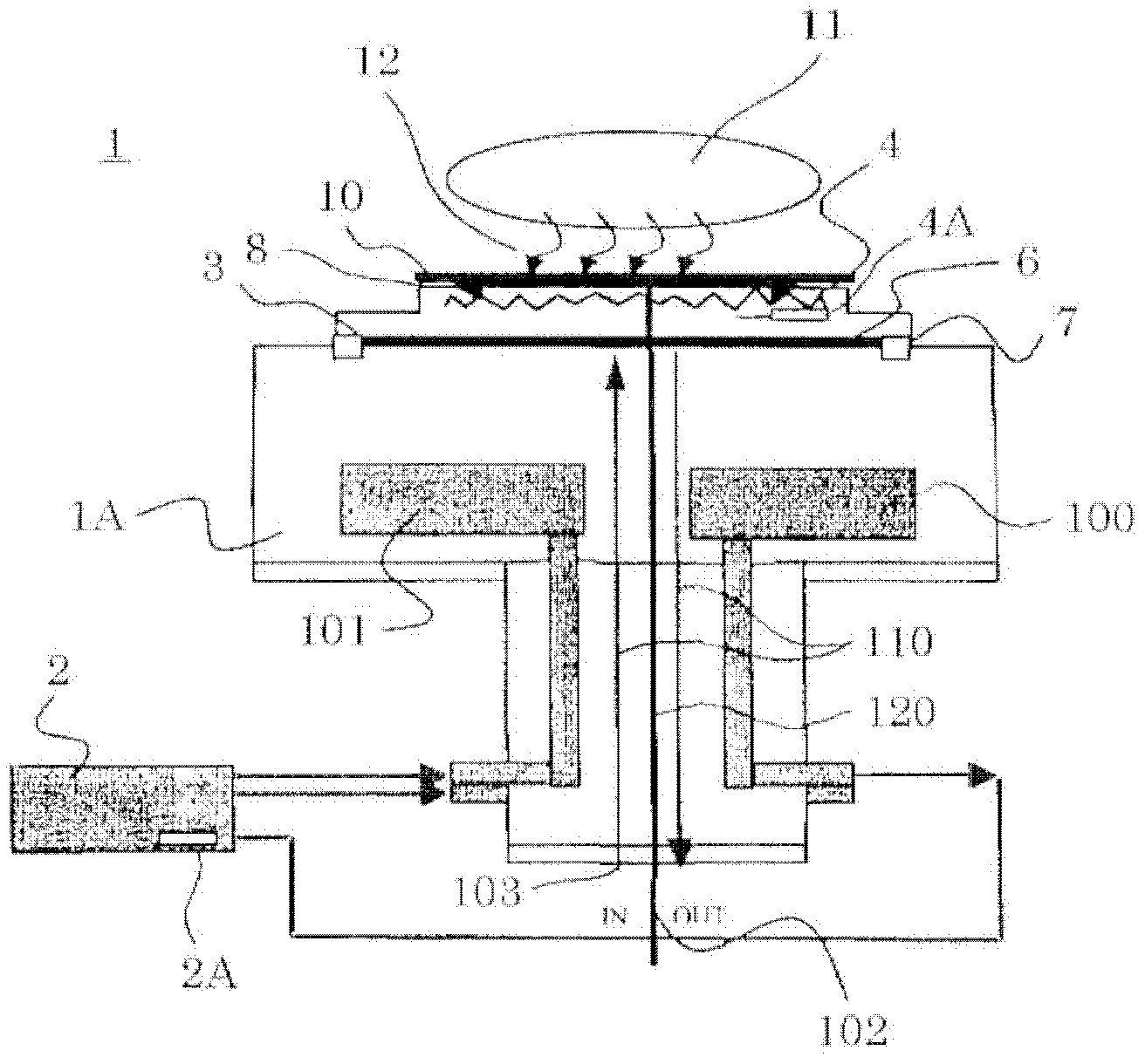
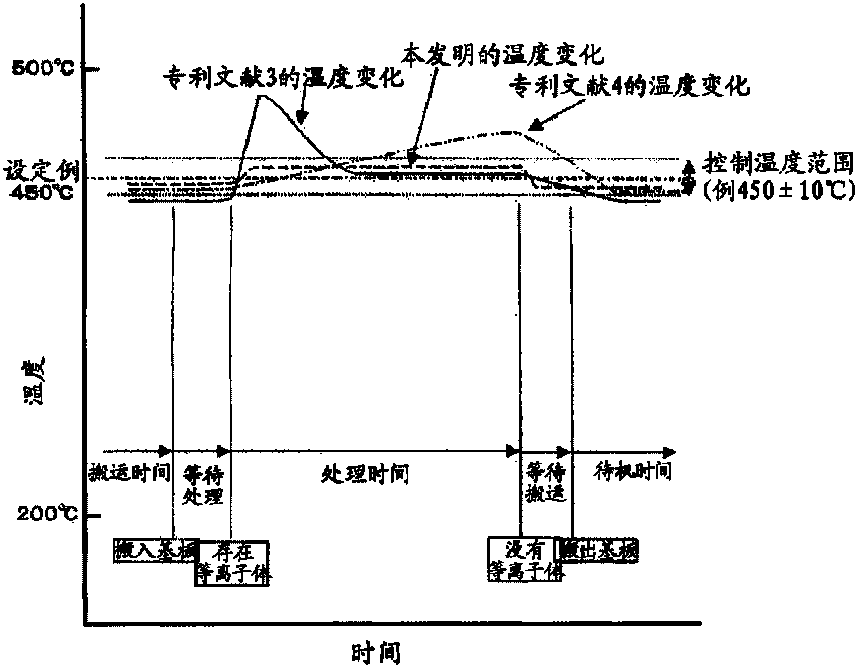
[0034] figure 1 It is a schematic diagram showing the first embodiment of the substrate holding device of the present invention. figure 2 It is an explanatory diagram showing the temperature change of the substrate holding device of the present invention in relation to the conventional temperature change.

[0035] Such as figure 1 As shown, the substrate holding device 1 according to the first embodiment is installed in a vacuum container (not shown) of a plasma processing device which is a representative device of a sputtering device. This substrate holding device 1 holds a substrate 10 by electrostatic attraction on an electrostatic chuck 3 disposed on the substrate holding side (upper part) of the holding device main body 1A.

[0036]The holding device main body 1A is, for example, a disk-shaped or cylindrical support member that supports a semiconductor wafer as a substrate 10 . A circulating medium flow path 100 through which a circulating medium (cooling medium) 10...

no. 2 Embodiment approach

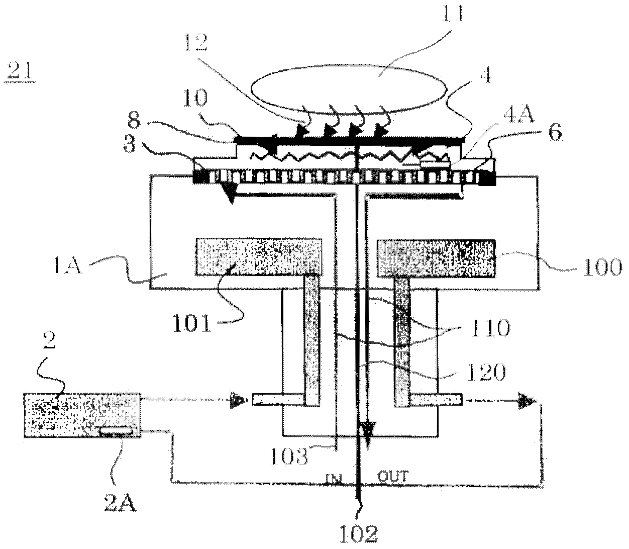
[0054] image 3 It is a schematic diagram showing the substrate holding device of the second embodiment. Figure 4 is a cross-sectional view showing the cross-sectional structure of the variable heat transfer energy member. The same reference numerals will be attached to the same components as those in the first embodiment for description.

[0055] The substrate holding device 21 of the second embodiment is a substrate holding device having the same specification as that of the first embodiment, in which the heat transfer energy variable member 6 defined and formed in the gap between the holding device main body 1A and the electrostatic chuck 3 is changed. constructed.

[0056] That is, the heat transfer energy variable member 6 in the second embodiment is divided and formed by arranging the first plate-shaped body 16 and the second plate-shaped body 17 facing each other. The first plate-shaped body 16 and the second plate-shaped body 17 has arc-shaped cooling fins 16A, 17A...

no. 3 Embodiment approach

[0059] Figure 5 It is a schematic diagram showing the third embodiment of the substrate holding device of the present invention. figure 2 It is an explanatory diagram showing the temperature change of the substrate holding device of the present invention in relation to the conventional temperature change.

[0060] Such as Figure 5 As shown, the substrate holding device 1 of the third embodiment is installed in a vacuum chamber (not shown) of a plasma processing device typified by a sputtering device. This substrate holding device 1 holds a substrate 10 by electrostatic attraction on an electrostatic chuck 3 disposed on the substrate holding side (upper part) of the holding device main body 1A.

[0061] The holding device main body 1A is, for example, a disk-shaped or cylindrical support member that supports a semiconductor wafer as a substrate 10 . A circulating medium flow path 100 through which a circulating medium (cooling medium) 101 flows is defined and formed in th...


PUM


Abstract

The invention provides a substrate temperature control method using a substrate holder. The substrate temperature control method comprises: (1) the first step of, before the start of a process, heating a substrate to a set temperature by using a heating unit in an electrostatic chuck and keeping the temperature constant at the set temperature until the process is started, without supplying the sealed gas into the gap between the holder and the electrostatic chuck; (2) the second step of, after the start of the process, when the temperature of the substrate is increased by a heat input from a plasma, supplying the sealed gas into the gap between the holder main body and the electrostatic chuck, maintaining the pressure of the sealed gas constant and deceasing the substrate temperature to the set temperature; and (3) the third step of, also after the start of the process, after the substrate temperature reaches the set temperature, adjusting the pressure of the sealed gas for heating the heating unit and the sealed gas supplied into the gap between the holder main body and the electrostatic chuck, and maintaining the substrate temperature at the set temperature.

Description

[0001] This application is a divisional application with an application date of July 9, 2009, an application number of 200910150087.X, and an invention name of a substrate holding device. technical field [0002] The present invention relates to a substrate holding device capable of holding a substrate by electrostatic adsorption in a vacuum container of a plasma processing apparatus and capable of controlling the temperature of the substrate. Background technique [0003] A substrate holding device (substrate support device) for holding a substrate (wafer) is provided in a vacuum container of a plasma processing device such as a sputtering device or an etching device, and usually can control the temperature of the substrate. [0004] For example, there has been proposed a substrate support device that includes a base member incorporating a heater or a cooler, and an electrostatic chuck that holds a wafer on its upper portion via a heat transfer sheet (see Patent Document 1)...

Claims


Application Information

Patent Timeline
Patent Type & Authority Applications(China)
IPC IPC(8): H01L21/67H01L21/683
CPCC23C14/50C23C16/4586C23C16/466H01L21/67109H01L21/6831
Inventor 吉田达彦金子一秋田中洋
Owner CANON ANELVA CORP
Why Eureka
Try Eureka