
Germanium ingots/wafers having low micro-pit density (mpd) as well as systems and methods for manufacturing same

A density, micro-pit technology, used in chemical instruments and methods, semiconductor/solid-state device manufacturing, crystal growth, etc., can solve problems such as reduction, low yield, and reduction in the number of useful crystals

Active Publication Date: 2012-02-15
AXT INC +1
View PDF2 Cites 3 Cited by
  • Summary
  • Abstract
  • Description
  • Claims
  • Application Information

AI Technical Summary

Problems solved by technology

For example, known crystal growth methods often produce crystals with excessive micropits or microcavities that lead to the appearance of flawed, defective devices and / or reduce the overall quality of crystals grown with such methods. useful quantity
This problem and the reduction in the number of useful crystals leads to a lower yield (yield)

Method used


Image

  • Germanium ingots/wafers having low micro-pit density (mpd) as well as systems and methods for manufacturing same
  • Germanium ingots/wafers having low micro-pit density (mpd) as well as systems and methods for manufacturing same
  • Germanium ingots/wafers having low micro-pit density (mpd) as well as systems and methods for manufacturing same

Examples


Embodiment Construction

[0017] The invention will now be described in detail, embodiments of which are illustrated in the accompanying drawings. The implementations presented below do not represent all implementations consistent with the claimed invention. Rather, they are merely some examples related to specific aspects of the invention. Wherever feasible, the same reference numbers will be used throughout the drawings to refer to the same or like parts.

[0018] The devices and methods are particularly applicable to devices and methods for germanium (Ge) crystal growth, and such devices and methods are described in this context. It should be understood, however, that the apparatus and method may have greater utility, as the apparatus and method may be used to produce other monocrystalline and / or polycrystalline ingots having low dimple densities.

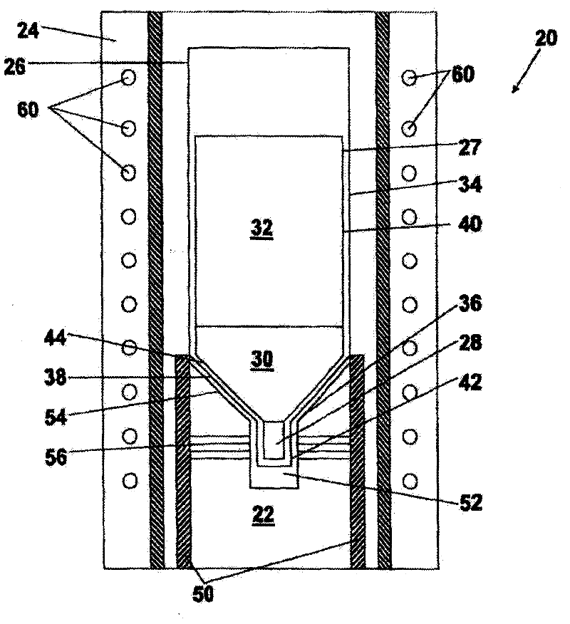
[0019] Figure 1A is a cross-sectional view of one embodiment of crystal growth apparatus 20 . This example apparatus may include a crucible support ...


PUM


Abstract

Systems and methods are disclosed for crystal growth including features of reducing micropit cavity density in grown germanium crystals. In one exemplary implementation, there is provided a method of inserting an ampoule with raw material into a furnace having a heating source, growing a crystal using a vertical growth process wherein movement of a crystallizing temperature gradient relative to the raw material / crucible is achieved to melt the raw material, and growing, at a predetermined crystal growth length, the material to achieve a monocrystalline crystal, wherein monocrystalline ingots having reduced micro-pit densities are reproducibly provided.

Description

[0001] Cross-references to relevant application data [0002] This application claims the benefit / priority of US Application No. 12 / 636,778, Publication No. US2011 / ______A1, filed December 13, 2009, which is hereby incorporated by reference in its entirety. technical field [0003] The systems and methods herein relate generally to single crystal germanium ingots / wafers, and in particular to the growth of ingots / wafers with reduced micropit density (MPD). Background technique [0004] Manufacturers of electronic and optoelectronic devices routinely require commercially grown, large and uniform individual semiconductor crystals that, when sliced ​​and polished, provide substrates for microelectronic device production. Growth of semiconductor crystals involves: heating a raw material to its melting point to produce a crystalline raw material melt; contacting the melt with high quality seed crystals; and allowing crystallization of the melt while in contact with the seed crysta...

Claims


Application Information

Patent Timeline
IPC IPC(8): C30B29/08C30B9/00H01L21/02
CPCC30B29/08C30B11/003C30B11/02Y10T428/24355Y10T117/1064
Inventor 刘卫国李晓
Owner AXT INC
Learn More