Wafer of planar optical waveguide splitter

A planar optical waveguide and splitter technology, applied in the direction of light guides, optics, instruments, etc., can solve the problems of large insertion loss temperature changes, poor etching uniformity, wafer waste, etc., to improve process unevenness performance, reduce polarization-dependent loss, and reduce product cost

Inactive Publication Date: 2012-02-22
宋齐望 +1
View PDF3 Cites 2 Cited by
  • Summary
  • Abstract
  • Description
  • Claims
  • Application Information

AI Technical Summary

Problems solved by technology

The main disadvantages of this type of optical splitter are: the loss is sensitive to the optical wavelength, and it is generally necessary to select devices according to the wavelength. This is a fatal flaw in the application process of triple play, because the optical signals transmitted in the triple play network have 1310nm, 1490nm , 1550nm and other wavelengths; the uniformity is poor, the 1*4 nominal maximum difference is about 1.5dB, and the difference above 1*8 is even larger, which cannot ensure uniform light splitting and may affect the overall transmission distance; the insertion loss varies greatly with temperature; Multi-channel splitters mostly rely on multiple 1*2 cascaded together and then packaged as a whole. The volume is larger, and the more the number of channels, the larger the volume, the lower the reliability, and the installation space is greatly limited.
[0006] In the traditional wafer manufacturing process, each chip unit is rectangular, and multiple identical rectangular units are arranged on the same wafer in the same direction (such as image 3 As shown), for this structure, for the optical splitter, due to the large difference in the number of channels at the input end and the output end, the etching uniformity becomes worse, the stress becomes larger, and the quality and performance of the device decrease; in addition, the wafer utilization rate Lower, and the more the number of shunts, the lower the utilization rate of the input terminal, and the more waste of wafers

Method used


Image

  • Wafer of planar optical waveguide splitter
  • Wafer of planar optical waveguide splitter
  • Wafer of planar optical waveguide splitter

Examples


Embodiment Construction

[0017] The preferred embodiments of the present invention will be described below in conjunction with the accompanying drawings. It should be understood that the preferred embodiments described here are only used to illustrate and explain the present invention, and are not intended to limit the present invention.

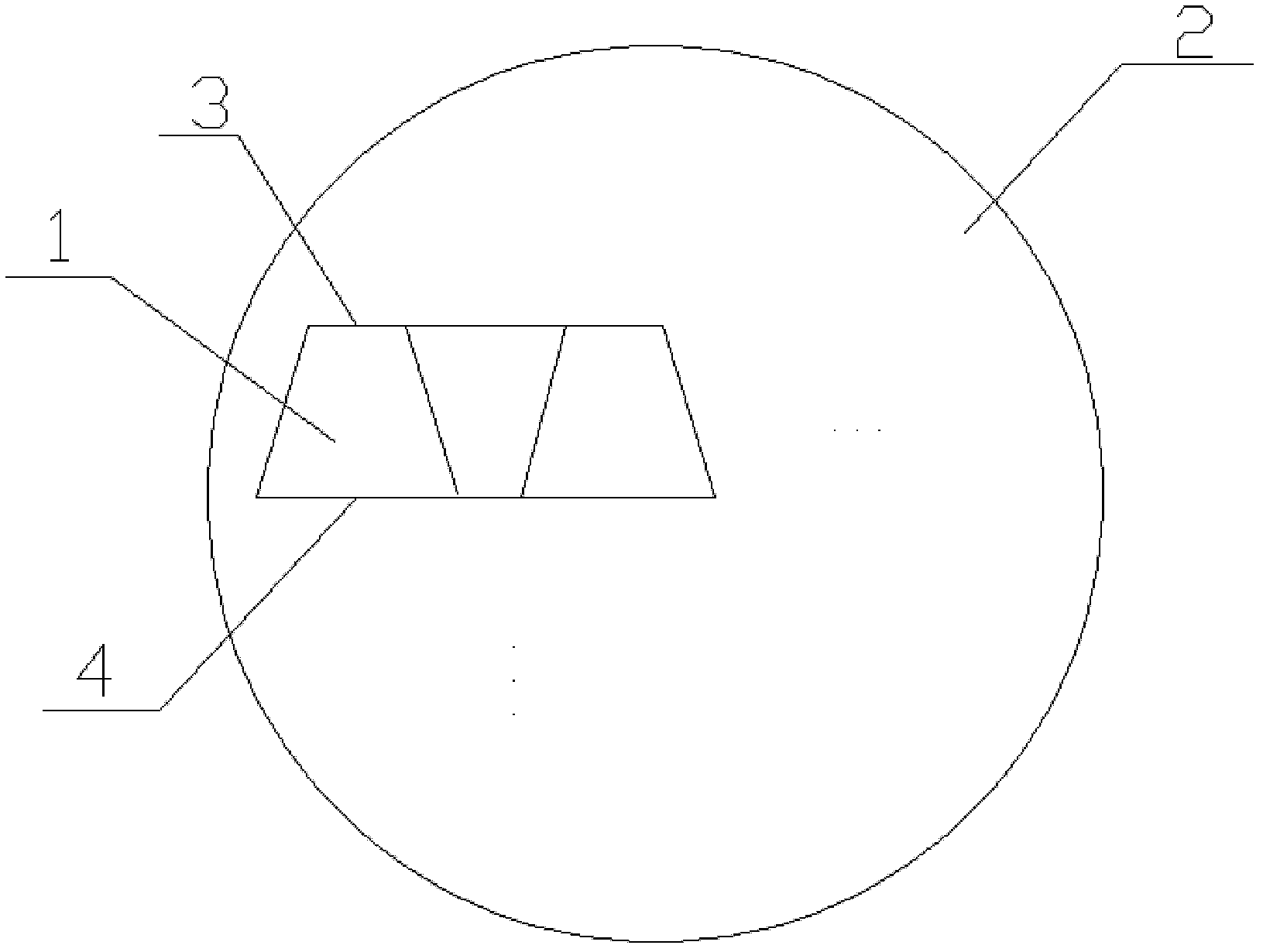
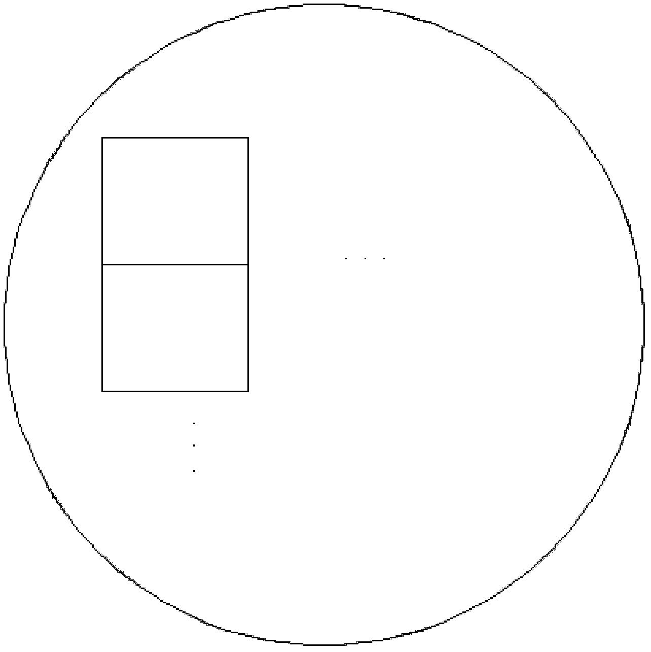
[0018] Such as figure 1 , figure 2 As shown, a wafer of planar optical waveguide splitters adopts planar optical waveguide splitter chips 1 in the shape of trapezoidal chips, and is arranged on the wafer 2 in reverse order.

[0019] The shape of the trapezoidal chip of the planar optical waveguide splitter chip 1 is an isosceles trapezoid, the upper bottom (short side) is used as the input terminal 3 , and the lower bottom (long side) is used as the output terminal 4 .

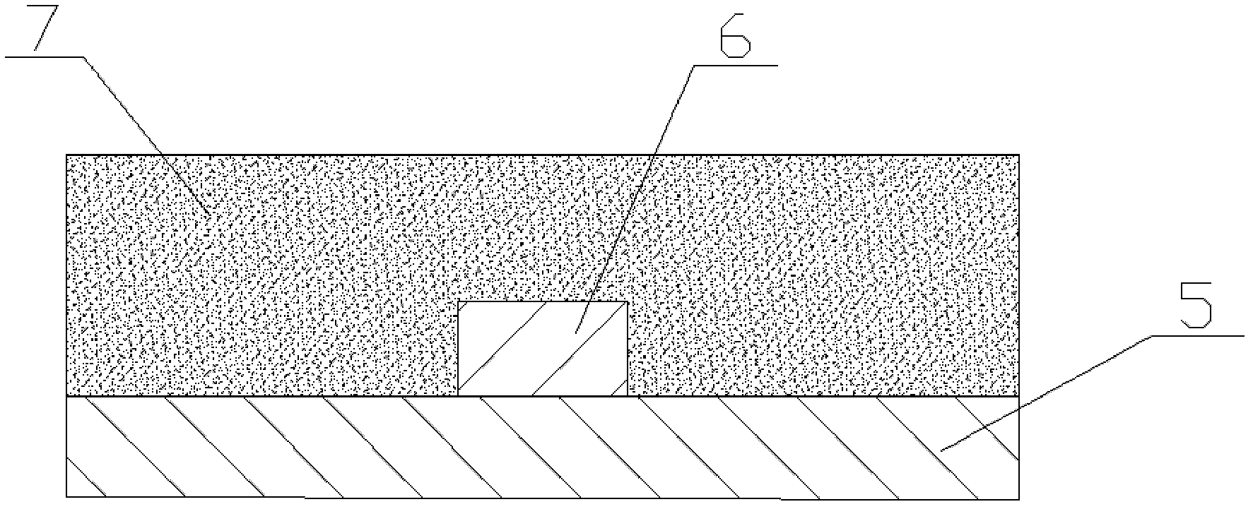
[0020] The substrate 5 of the planar optical waveguide splitter chip 1 is silicon dioxide.

[0021] The specific process is as follows:

[0022] The waveguide core 6 is directly grown on the si...


PUM


Abstract

The invention provides a wafer of a planar optical waveguide splitter. Trapezoidal planar optical waveguide splitter chips are adopted, which are arranged on the wafer in the manner of inversed pairs in succession. By utilizing the wafer of the planar optical waveguide splitter provided by the invention, the nonuniformity of a process caused by the structure is improved, thus the stress is greatly reduced, and the quality of a device is improved; more chip units are arranged on the wafers with the same sizes; and the utilization rate of the wafers is higher, as a larger number of channels are provided, thus improving the chip production value of a single wafer, and lowering the production cost; and in addition, silicon oxide is adopted as a substrate, thus omitting the step that a lower clapping layer of the silicon oxide grows on a silicon substrate in the traditional semiconductor process, shortening the growth cycle of the product, and lowering the production cost; and the substrate and the lower clapping layer are made of the same material, thus eliminating the stress influence of the substrate on the device, and lowering the polarization dependent loss of the device.

Description

technical field [0001] The invention belongs to the field of optical passive devices, in particular to a planar optical waveguide splitter wafer. Background technique [0002] PON / FTTP technology can provide higher bandwidth for the access network. The optical splitter is the core optical device of FTTH. The optical splitter controls the distribution of optical power from the central office (CO) to the local distribution frame. At present, there are two main types of optical splitters: the fused fiber splitter (Fused Fiber Splitter) produced by the traditional tapered coupler process, and the planar optical waveguide optical splitter (Fused Fiber Splitter) produced based on optical integration technology and semiconductor technology. PLC Splitter). [0003] Fused tapered optical splitter clamps two or more optical fibers together, melts and stretches them on a fusion tapered machine, and monitors the change of splitting ratio in real time, and stops stretching when the spli...

Claims


Application Information

Patent Timeline
Patent Type & Authority Applications(China)
IPC IPC(8): G02B6/125
Inventor 宋齐望孙麦可
Owner 宋齐望
Why Eureka
Try Eureka