
Semiconductor device

A semiconductor and N-type semiconductor technology, applied in semiconductor devices, semiconductor/solid-state device manufacturing, electric solid-state devices, etc., can solve the problems of high manufacturing costs and achieve the effect of reducing costs and time

Active Publication Date: 2012-02-22
ROHM CO LTD
View PDF8 Cites 5 Cited by
  • Summary
  • Abstract
  • Description
  • Claims
  • Application Information

AI Technical Summary

Problems solved by technology

However, in this method, since heat treatment at a high temperature of 1000° C. is required, the manufacturing cost becomes high

Method used


Image

  • Semiconductor device
  • Semiconductor device
  • Semiconductor device

Examples


Embodiment 1~12 and comparative example 1

[0253] In order to prove the reduction effect of on-resistance and drain leakage current, Examples 1 to 12 and Comparative Example 1 were carried out in the following manner.

Embodiment 1

[0255] An N-type impurity concentration of 7×10 is formed on a SiC substrate by epitaxial growth. 15 cm - 3 SiC epitaxial layer. Then, through the injection energy of 300keV and 7×10 13 cm -2 Doping the surface layer of the SiC epitaxial layer with Al to form a P-type region (main region) by using a single-stage ion implantation method with a high dose.

[0256] From this, it is obtained with Figure 22 The impurity concentration profile is shown for the P-type region. That is to say, the P-type region has a distance from the surface of the SiC epitaxial layer 42 The P-type impurity concentration in the part below (80nm) is 1×10 18 cm -3 The following impurity concentration distribution.

Embodiment 2

[0258] An N-type impurity concentration of 7×10 is formed on a SiC substrate by epitaxial growth. 15 cm - 3 SiC epitaxial layer. Then, through the injection energy of 300keV and 6×10 13 cm -2 Doping the surface layer of the SiC epitaxial layer with Al to form a P-type region (main region) by using a single-stage ion implantation method with a high dose.

[0259] From this, it is obtained with Figure 23 The impurity concentration profile is shown for the P-type region. That is to say, the P-type region has a distance from the surface of the SiC epitaxial layer 42 The P-type impurity concentration in the following part is 1×10 18 cm -3 The following impurity concentration distribution.


PUM

PropertyMeasurementUnit
On resistanceaaaaaaaaaa
Peak concentrationaaaaaaaaaa

Abstract

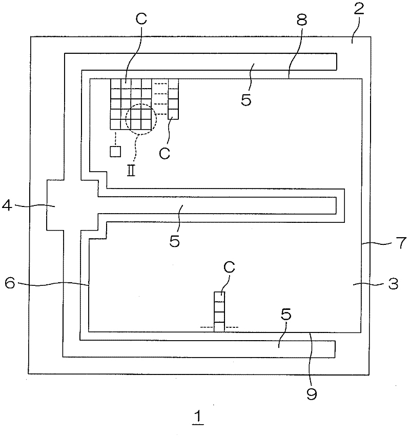
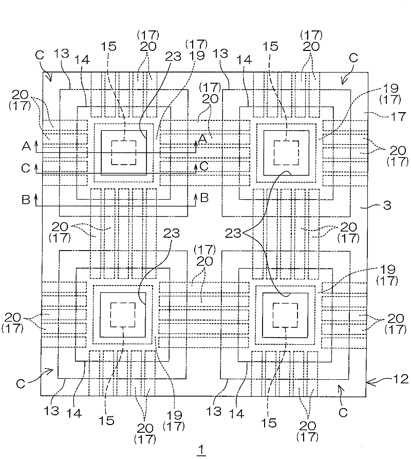
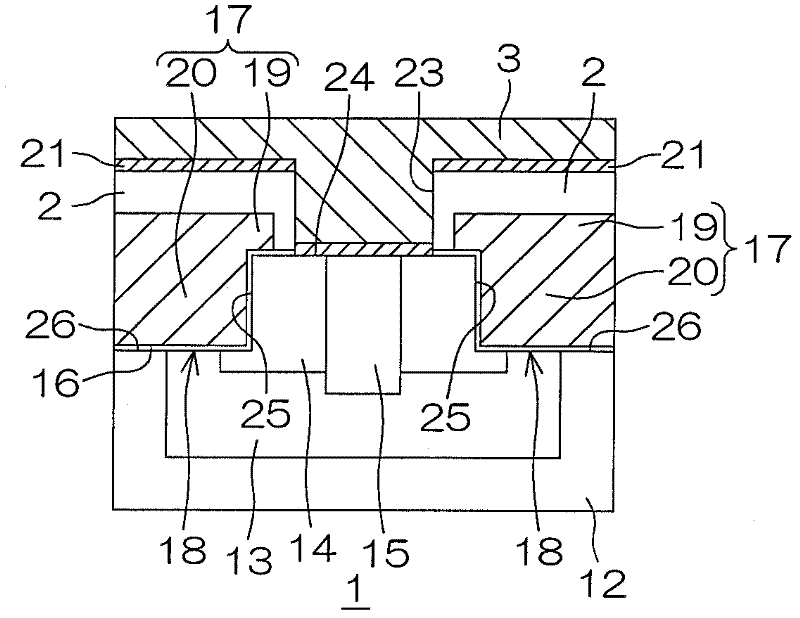
A semiconductor device including a semiconductor layer of a first conductivity type; a plurality of body regions of a second conductivity type, each formed in a region extending from the surface of the semiconductor layer to a halfway portion of the same in the thickness direction, and each spaced apart from each other in a direction perpendicular to the thickness direction; source regions of the first conductivity type, each formed on the surface layer part of each body region and spaced away from the edges of each body region; a gate insulating film formed on the semiconductor layer; and gate electrodes formed on the gate insulating film. In the semiconductor layer, trenches extending between two neighboring source regions are formed by digging from the surface of the semiconductor layer, the inside surface of the trenches are covered by the gate insulating film, and the gate electrodes comprise surface-facing parts, which face the surface of the semiconductor layer, and buried parts, which are buried in the trenches.

Description

technical field [0001] The present invention relates to a semiconductor device including a transistor. Background technique [0002] SiC (silicon carbide) semiconductors are excellent in dielectric breakdown resistance, thermal conductivity, etc., and are attracting attention as semiconductors suitable for use in inverters and the like of hybrid vehicles. [0003] For example, an inverter using a SiC semiconductor has a MOSFET (Metal Oxide Semiconductor Field Effect Transistor). Such a SiC semiconductor device includes a SiC substrate and an N-type SiC epitaxial layer stacked on the SiC substrate. In the surface layer portion of the SiC epitaxial layer, a plurality of P-type body regions (well regions) are formed at intervals from each other. An N-type source region is formed in the surface portion of each body region at a distance from the periphery of the body region. On the SiC epitaxial layer, a gate electrode made of N-type polysilicon (polysilicon doped with N-type ...

Claims


Application Information

Patent Timeline
IPC IPC(8): H01L29/78H01L21/28H01L21/336H01L29/12H01L29/739
CPCH01L29/045H01L29/1095H01L29/1608H01L29/4236H01L29/42376H01L29/4238H01L29/45H01L29/66068H01L29/7811H01L29/7813H01L2224/0603H01L29/1045H01L29/7816
Inventor 中野佑纪箕谷周平三浦峰生
Owner ROHM CO LTD
Features
  • Generate Ideas
  • Intellectual Property
  • Life Sciences
  • Materials
  • Tech Scout
  • Unparalleled Data Quality
  • Higher Quality Content
  • 60% Fewer Hallucinations
Learn More