Method for interconnecting electrodes of MEMS (micro electro mechanical system) device based on SOI (silicon-on-insulator)

A device and electrode technology, applied in the field of microelectronic machinery, can solve the problems of complex process technology, high technical difficulty, and low yield

Active Publication Date: 2012-03-07
EAST CHINA INST OF OPTOELECTRONICS INTEGRATEDDEVICE
View PDF8 Cites 24 Cited by
  • Summary
  • Abstract
  • Description
  • Claims
  • Application Information

AI Technical Summary

Problems solved by technology

[0005] The purpose of the present invention is to solve the defects of high technical difficulty, complex process technology, and low yield in the prior art using dielectric filling, planarization and other technological means, and to provide a MEMS device electrode interconnection method based on SOI

Method used


Image

  • Method for interconnecting electrodes of MEMS (micro electro mechanical system) device based on SOI (silicon-on-insulator)
  • Method for interconnecting electrodes of MEMS (micro electro mechanical system) device based on SOI (silicon-on-insulator)
  • Method for interconnecting electrodes of MEMS (micro electro mechanical system) device based on SOI (silicon-on-insulator)

Examples


Embodiment Construction

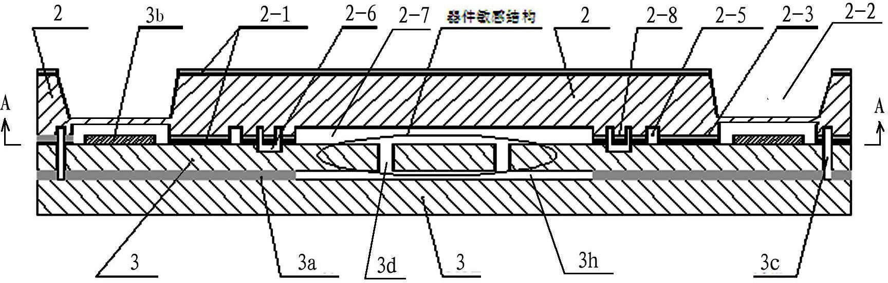
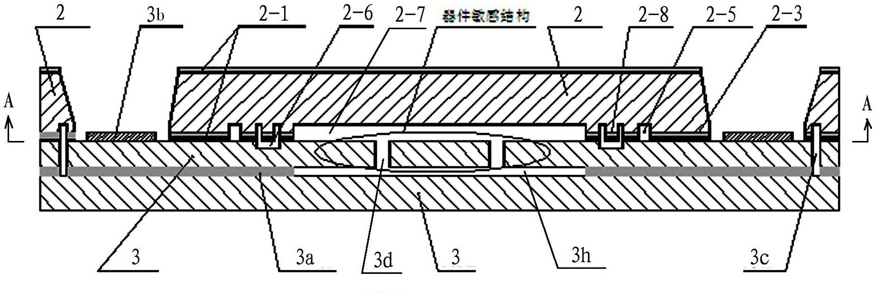
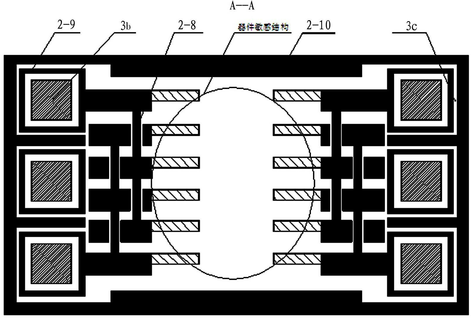
[0029] The method for interconnecting electrodes of SOI-based MEMS devices will be described below by taking a high-precision, high-performance capacitive MEMS device as an example.

[0030] (1) Fabrication of silicon cover plate

[0031] Figure 2-1 to Figure 2-4 in Figure 2 show the main process of silicon cover plate production, and the specific description is as follows:

[0032] (1) Growth of silicon dioxide: grow a layer of SiO on both sides of the cleaned double-sided polished silicon wafer 2 2 Thermal oxide layer 2-1. In the thermal oxidation furnace, the following parameters were used: 30 min O 2 (heating up) +10 minutes dry O 2 (920°C) +660 minutes wet O 2 (1100°C) +10 minutes dry O 2 (920°C) +N 2 (cooling), growing SiO 2 The thickness is more than 2 μm. The purpose of this oxide layer is to act as electrical isolation and as a masking layer for deep hole etching, such as Figure 2a shown.

[0033] (2) Making deep holes: use a photolithography process on the...


PUM

PropertyMeasurementUnit
thicknessaaaaaaaaaa
thicknessaaaaaaaaaa

Abstract

The invention relates to a method for interconnecting electrodes of an MEMS (micro electro mechanical system) device based on an SOI (silicon-on-insulator). In the method, a metal interconnection lead (2-8) and various electric isolation grooves (2-5, 2-6) are made on a silicon cover plate (2); and then, a structure layer (3) of the MEMS device is stuck with the silicon cover plate (2) through gold-silicon eutectic bonding, so that the electrodes of the MEMS device are interconnected together through the metal lead on the cover plate and led out to metal pressure welding points. The method provided by the invention overcomes the technical problems caused by the prior art adopting the techniques such as medium filling, flattening and the like, simplifies the techniques, is easy to operate, and is suitable for manufacturing various SOIMEMS devices.

Description

technical field [0001] The invention belongs to the technical field of microelectronic machinery. It relates to an SOI-based MEMS device electrode interconnection method. Background technique [0002] SOI technology was developed rapidly in the 1980s and has been called the silicon integration technology of the 21st century. With the gradual maturity of SOI process technology and the continuous reduction of the cost of SOI silicon wafers, the application field of SOI has gradually expanded, and it has been widely used in the field of MEMS in recent years. At present, foreign SOI technology is relatively mature. Many research institutions and companies have adopted SOI technology for MEMS devices, such as pressure sensors, inertial devices, and high-temperature sensors. The French company Tronic has successfully developed the SOI process and has been processing MEMS for many years. France's MEMSCAP company has developed a MEMS process technology called SOIMUMP, which is u...

Claims


Application Information

Patent Timeline
Patent Type & Authority Applications(China)
IPC IPC(8): B81C1/00
Inventor 方澍郭群英徐栋黄斌陈博王祖民
Owner EAST CHINA INST OF OPTOELECTRONICS INTEGRATEDDEVICE
Why Eureka
Try Eureka