

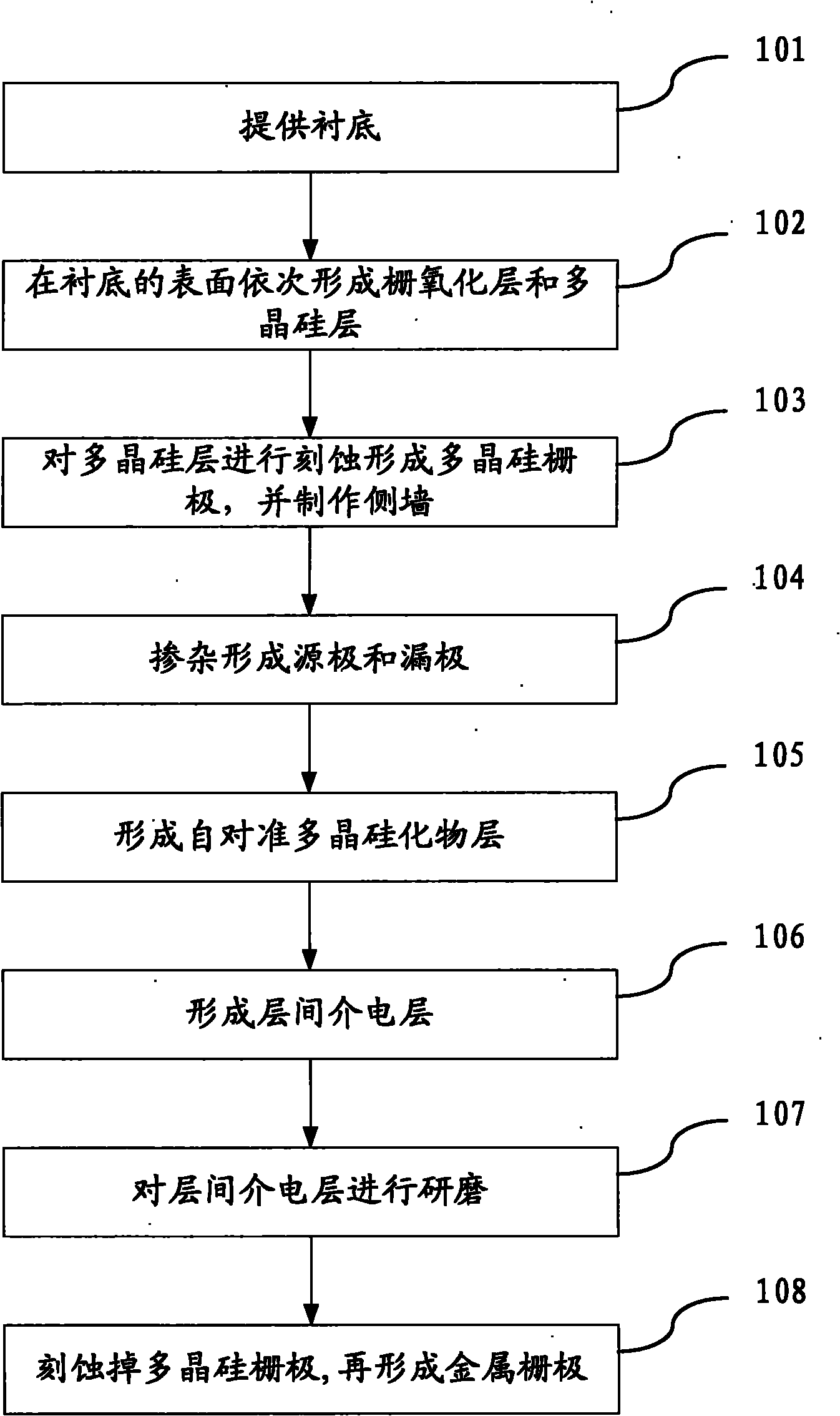
Method for producing semiconductor device
A technology for semiconductors and devices, applied in the field of manufacturing semiconductor devices, can solve the problems of destroying the gate oxide layer, different depths of etching, and inability to grind off silicides.
- Summary
- Abstract
- Description
- Claims
- Application Information
AI Technical Summary
Problems solved by technology
Method used
Image

Examples
Embodiment Construction
[0032] In the following description, numerous specific details are given in order to provide a more thorough understanding of the present invention. It will be apparent, however, to one skilled in the art that the present invention may be practiced without one or more of these details. In other examples, some technical features known in the art are not described in order to avoid confusion with the present invention.
[0033] In order to provide a thorough understanding of the present invention, detailed steps will be set forth in the following description to illustrate how the present invention proposes a method of fabricating a semiconductor device. Obviously, the practice of the invention is not limited to specific details familiar to those skilled in the semiconductor arts. Preferred embodiments of the present invention are described in detail below, however, the present invention may have other embodiments besides these detailed descriptions.
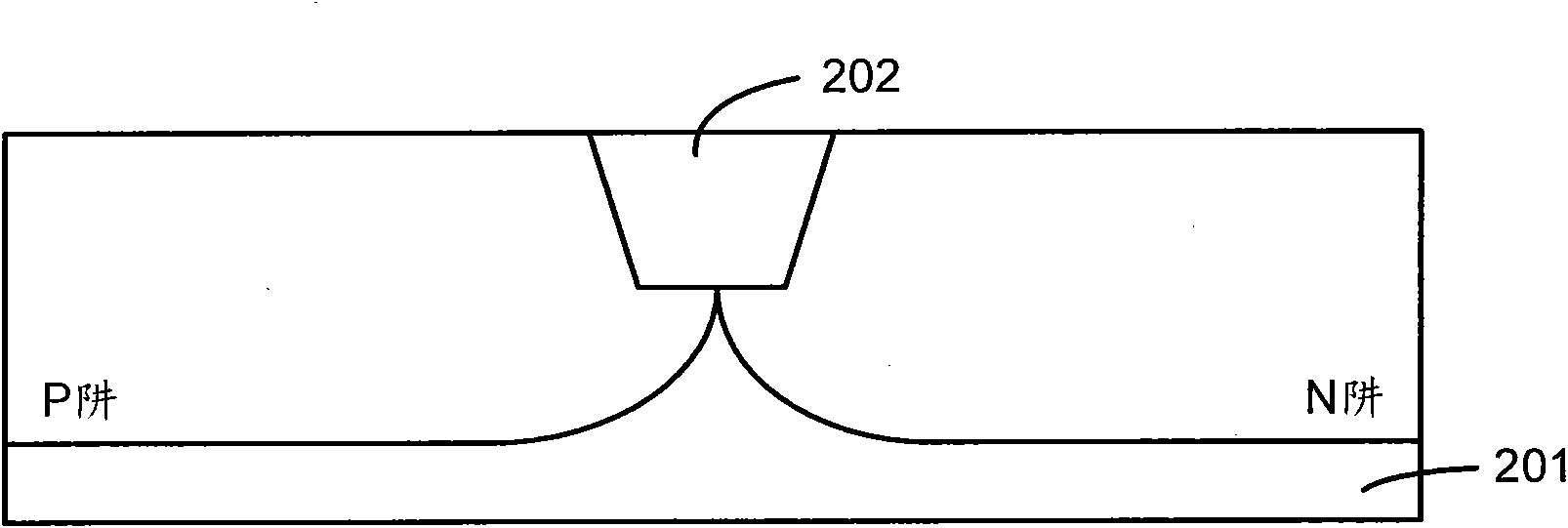
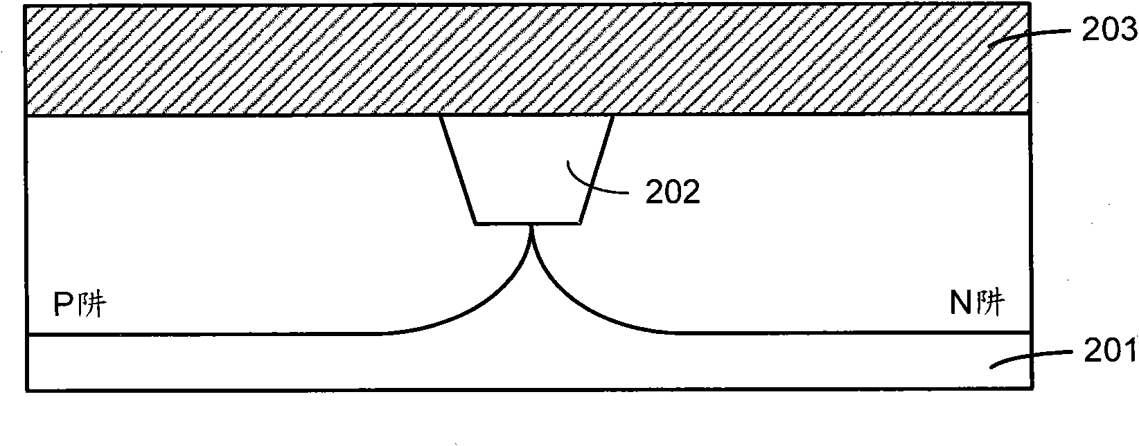
[0034] Combine the follow...
PUM
| Property | Measurement | Unit |
|---|---|---|
| Thickness | aaaaa | aaaaa |
| Thickness | aaaaa | aaaaa |
Abstract
Description
Claims
Application Information