Manufacturing method for silicon germanium heterojunction bipolar transistors

A heterojunction bipolar and transistor technology, applied in semiconductor/solid-state device manufacturing, semiconductor devices, electrical components, etc., can solve the problems of reduced polysilicon emitter size, high quasi-accuracy requirements, and complex processes. The effect of reducing rb and increasing device Fmax

Active Publication Date: 2012-04-04
SHANGHAI HUAHONG GRACE SEMICON MFG CORP
View PDF5 Cites 10 Cited by
  • Summary
  • Abstract
  • Description
  • Claims
  • Application Information

AI Technical Summary

Problems solved by technology

In order to reduce the resistance of the intrinsic base region at the bottom of the dielectric layer of the emitter window, the usual method is to form a transistor through a self-aligned process, but this method makes the process very complicated
Another method is to reduce the resistance of the intrinsic base region at the bottom of the emission region window dielectric layer by reducing the width of the emission region extending out of the emission region window, that is, reducing the width of the emission region window dielectric layer. It has a better effect, but the price is that the emitter polysilicon lithography must use a very advanced lithography machine, because on the one hand, the size of the polysilicon emitter needs to be reduced, and on the other hand, the alignment accuracy is also very high.

Method used


Image

  • Manufacturing method for silicon germanium heterojunction bipolar transistors
  • Manufacturing method for silicon germanium heterojunction bipolar transistors
  • Manufacturing method for silicon germanium heterojunction bipolar transistors

Examples


Embodiment Construction

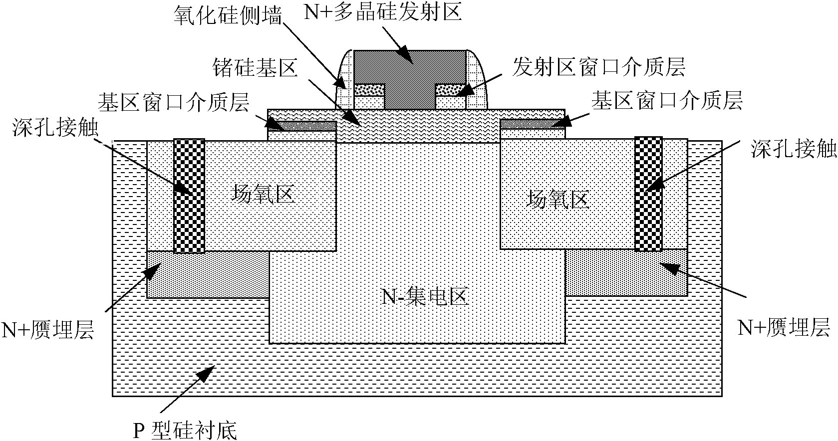
[0027] like figure 2 As shown, it is a flowchart of a method according to an embodiment of the present invention. like Figure 3-Figure 14 As shown, it is a schematic structural diagram of a silicon germanium heterojunction bipolar transistor in each step of the method according to the embodiment of the present invention.

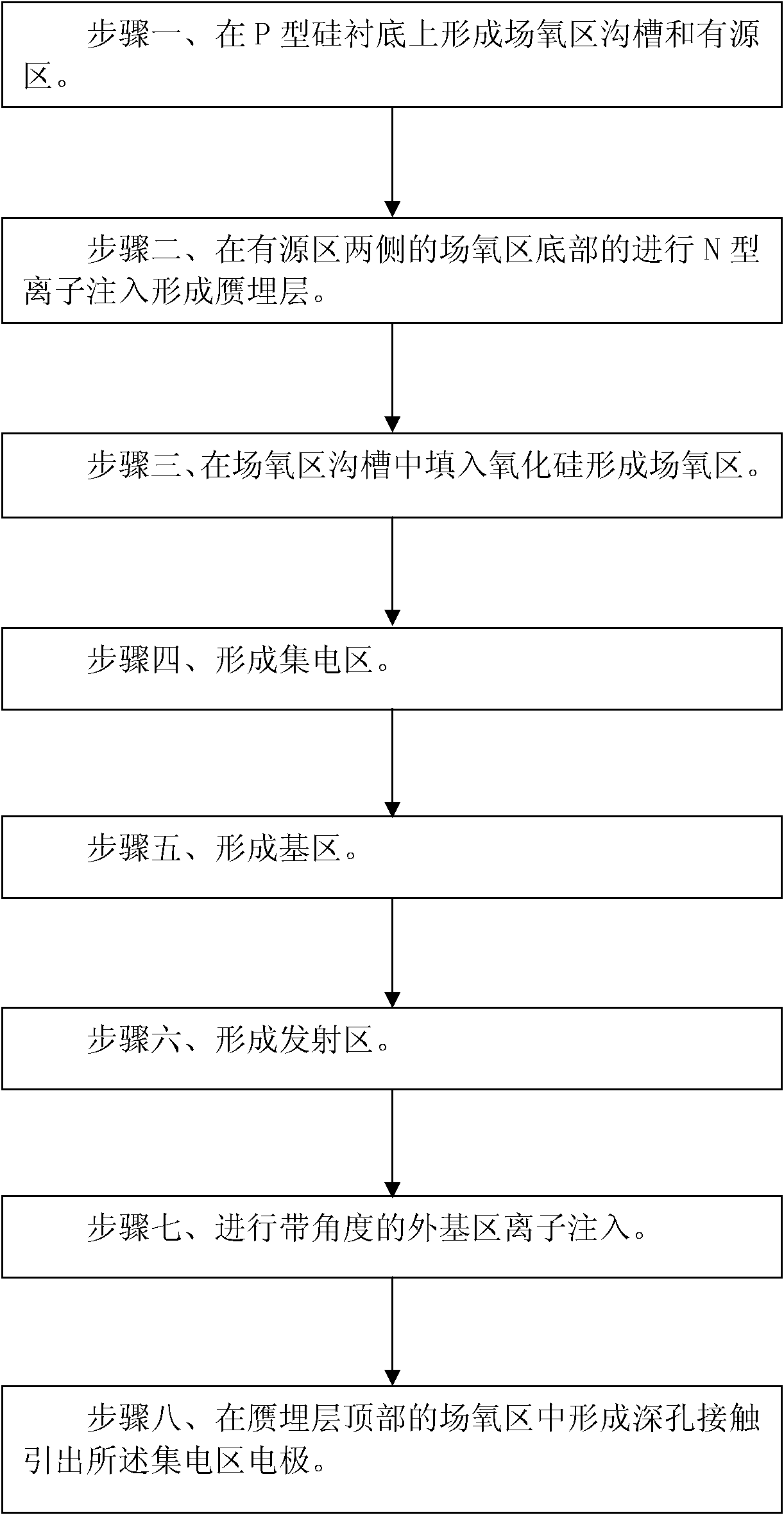
[0028] The manufacturing method of the silicon germanium heterojunction bipolar transistor according to the embodiment of the present invention includes the following steps:

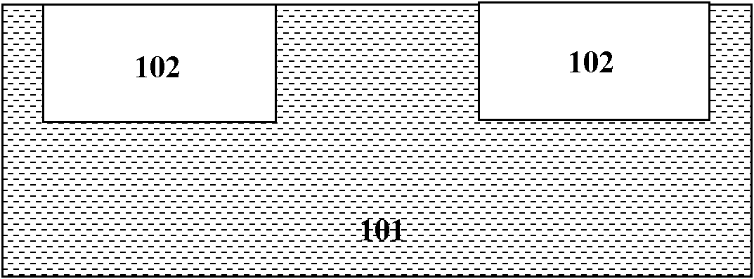
[0029] Step one, as image 3 As shown, trenches and active regions are formed on the P-type silicon substrate 101 for the field oxide region 102 .

[0030] Step 2, forming a pseudo buried layer 103 . First, as Figure 4 As shown, the pseudo-buried layer 103 region is defined by photolithography, that is, photoresist is used to form a pseudo-buried layer protection window during ion implantation of the pseudo-buried layer 103, and the edge of the pseudo-buried layer protection wind...


PUM


Abstract

The invention discloses a manufacturing method for silicon germanium heterojunction bipolar transistors. After an emitter region is formed, ion implantation is performed in a base region by means of angular external base region ion implantation process, ions for external base region ion implantation are boron ions, implantation dosage ranges from 1e15cm-2 to 1e16cm-2, implantation energy ranges from 5KeV to 30KeV, and implantation angle ranges from 5 degrees to 30 degrees. Due to the implantation angle of external base region ion implantation, boron impurities can be doped in the base region outside a contact region of the emitter region and the base region. Resistance of the base region of a device can be further reduced without reducing dimension of the device and frequency characteristics of the device can be improved by the manufacturing method for silicon germanium heterojunction bipolar transistors.

Description

technical field [0001] The invention relates to a method for manufacturing a semiconductor integrated circuit, in particular to a method for manufacturing a silicon germanium heterojunction bipolar transistor. Background technique [0002] With the increasing maturity of silicon germanium (SiGe) technology, the integration of radio frequency circuits is becoming more and more common, and radio frequency reception, radio frequency transmission, and switches tend to be integrated. Therefore, a low noise amplifier (LNA) that amplifies the received signal and amplifies the power of the transmitted signal Amplifiers (PA) should be fabricated on the same chip. In order to increase the operating frequency of bipolar transistor devices, it is necessary to maximize the maximum oscillation frequency of bipolar transistor devices (F max ). Its calculation formula is: [0003] F max = ( ...

Claims


Application Information

Patent Timeline
Patent Type & Authority Applications(China)
IPC IPC(8): H01L21/331H01L29/737H01L21/265
CPCH01L21/26586H01L21/26513H01L29/7378H01L29/66242H01L29/0821
Inventor 陈帆陈雄斌周正良
Owner SHANGHAI HUAHONG GRACE SEMICON MFG CORP
Why Eureka
Try Eureka