

Method for preparing ordered micron/nano structure array of conducting polymer
A technology of conductive polymers and nanostructures, applied in the field of polymer materials, to achieve the effects of easy operation, fast migration, and reasonable and simple preparation methods
- Summary
- Abstract
- Description
- Claims
- Application Information
AI Technical Summary
Problems solved by technology
Method used
Image

Examples
Embodiment 1
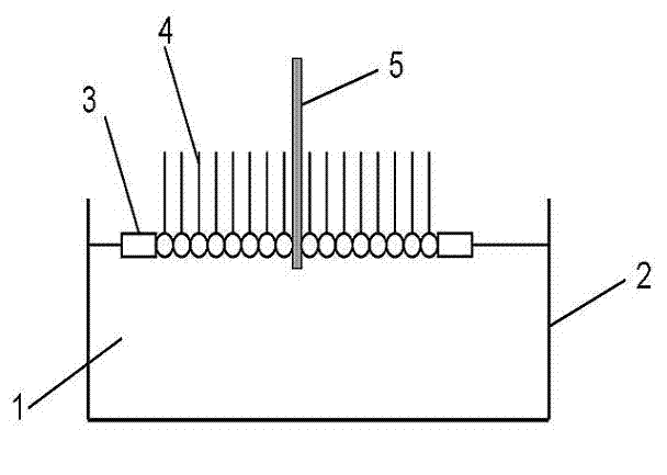
[0044] exist figure 1 The middle LB film tank is an ultra-pure aqueous solution. When a certain concentration of dodecyl-3,4-ethylenedioxythiophene / chloroform solution mixture is added to the surface of the ultra-pure aqueous solution, the monomer molecules can be effectively in the gas / After the chloroform volatilizes, control the sliding barrier 5 to compress the monomolecular film at a certain speed, keep the molding pressure constant for a period of time after reaching the required surface pressure, and then control the substrate to transfer the monomolecular film to the substrate at a certain speed. The surface of the chip and the surface of the substrate are treated with hydrophilicity.
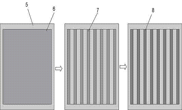
[0045] exist figure 2 in, by figure 1 The obtained polymer monomer ordered film obtains an ordered array structure of monomer micro / nano structures by means of electron beam etching.
[0046] exist figure 2 In the process, the ordered array of monomeric micro / nanostructures is fu...
Embodiment 2
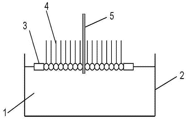
[0055] Such as figure 2 , the monomer material is octadecyl-3,4-ethylenedioxythiophene, and the surface of the substrate is treated with hydrophobicity.
[0056] The preparation process of the ordered nanowire structure array is similar to Embodiment 1. Since the monomer material is octadecyl-3,4-ethylenedioxythiophene, polyoctadecyl-3,4-vinyldioxythiophene is obtained. Oxythiophene Conductive Polymer Nanowire Structure Arrays.
[0057] The etching line width is 250 nanometers, thereby obtaining a polyoctadecyl-3,4-ethylenedioxythiophene nanowire ordered structure array with a width of 250 nanometers.
Embodiment 3
[0059] Such as figure 2 , the monomer material is eicosyl-3,4-ethylenedioxythiophene, and the surface of the substrate is treated with hydrophobicity.
[0060] The preparation process of the ordered nanowire structure array is similar to Embodiment 1. Since the monomer material is eicosyl-3,4-ethylenedioxythiophene, polyeicosyl-3,4-ethylenedioxythiophene is obtained. Oxythiophene Conductive Polymer Nanowire Structure Arrays.
[0061] The etching line width is 250 nanometers, thereby obtaining a polyeicosyl-3,4-ethylenedioxythiophene nanowire ordered structure array with a width of 250 nanometers.
PUM
 Abstract
Description
Claims
Application Information