

Method for improving breakdown voltage of N-groove laterally diffused metal oxide semiconductor (LDMOS)
A technology of breakdown voltage and multiple injections, applied in the manufacturing of circuits, electrical components, semiconductor/solid-state devices, etc., can solve problems such as simultaneous achievement, and achieve the effect of increasing withstand voltage and reducing impact ionization
- Summary
- Abstract
- Description
- Claims
- Application Information
AI Technical Summary
Problems solved by technology
Method used
Image

Examples
Embodiment Construction
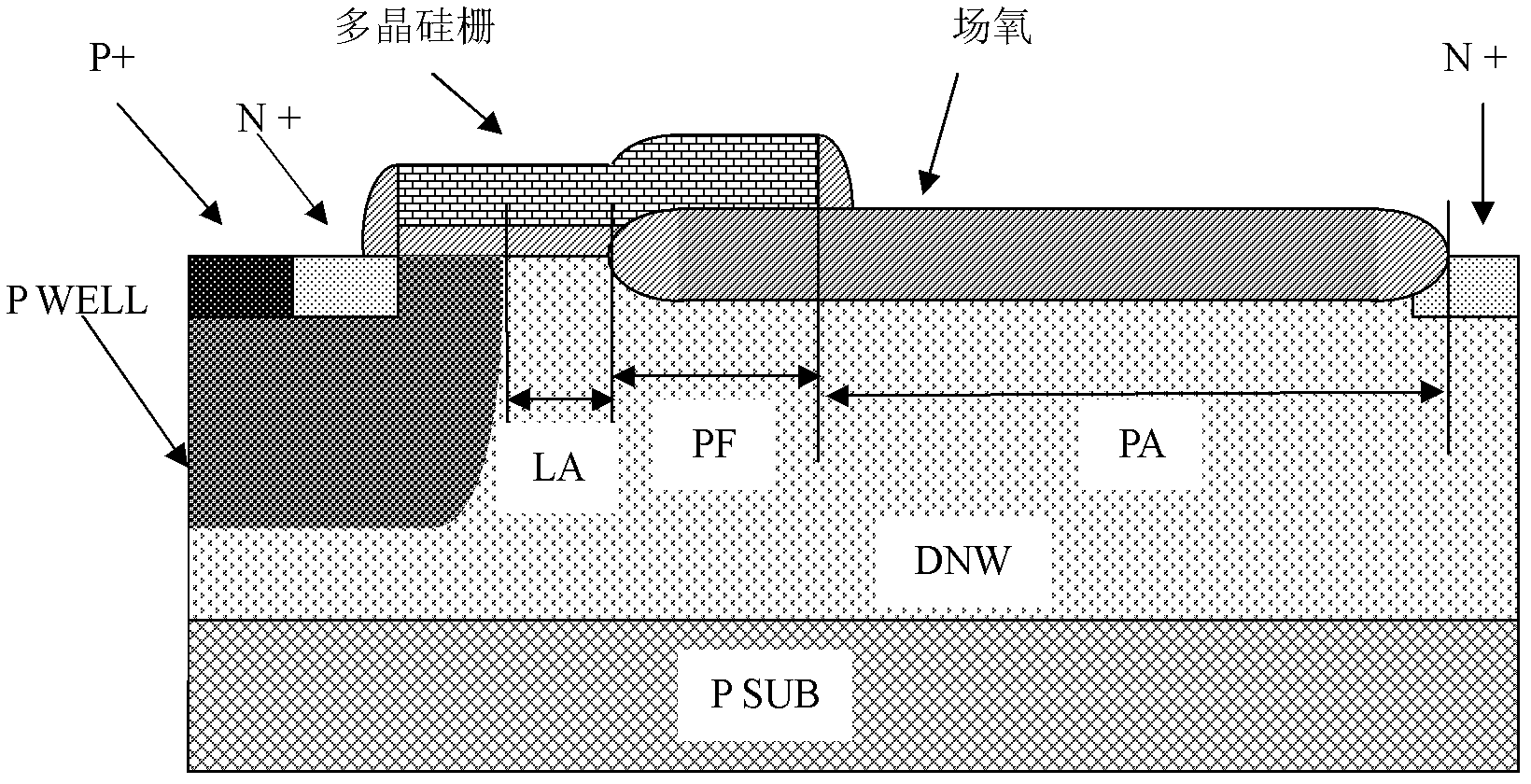
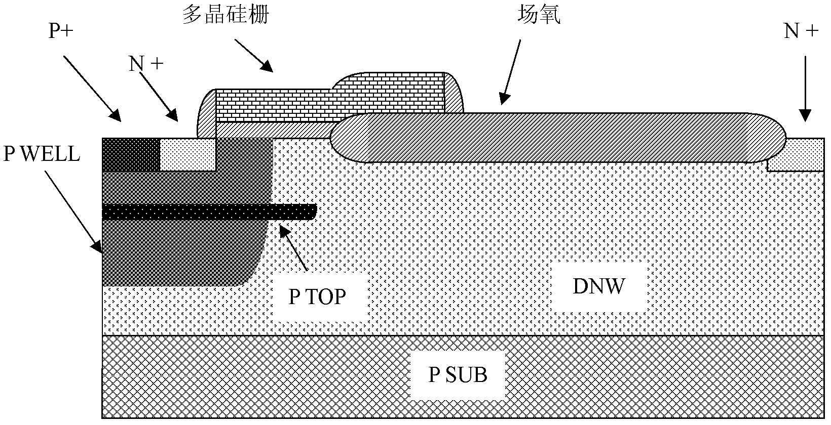
[0033] In the present invention, the PTOP is placed under the source terminal and the gate oxide, so as to reduce the electric field intensity at the bird's beak, thereby optimizing the OFF BV and ON BV of the device.
[0034] Such as figure 2 As shown, the present invention implants PTOP at the source and extends all the way under the gate oxide in the deep N-well DNW. By optimizing the length of PTOP below the gate oxide, the OFF BV and ON BV of the device can be optimized.
[0035] 1. Fabrication of deep N well DNW: Phosphorus is implanted on the P-type substrate P SUB with an energy of 100keV-300keV and a dose of 10 11 ~10 14 cm -2 . Then it is formed by high temperature promotion. The temperature is 1000° C. to 1200° C., and the time is 100 minutes to 500 minutes.
[0036] 2. Fabrication of polysilicon gate and polysilicon field plate: After the growth of the gate oxide layer is completed, a layer of polysilicon is deposited. Then define the position of polysilico...
PUM
 Abstract
Description
Claims
Application Information