High-efficient four solar cell and manufacturing method thereof

A technology for solar cells and manufacturing methods, which is applied in circuits, photovoltaic power generation, electrical components, etc., can solve problems such as current recombination loss, complex post-processing, and lower efficiency, so as to reduce dislocation density, broaden spectral absorption range, and high crystallinity. The effect of grid quality

Inactive Publication Date: 2012-04-11
XIAMEN SANAN OPTOELECTRONICS TECH CO LTD
View PDF5 Cites 12 Cited by
  • Summary
  • Abstract
  • Description
  • Claims
  • Application Information

AI Technical Summary

Problems solved by technology

For stacked cells, the efficiency of each sub-cell is the highest when the currents of each sub-cell are equal, and the current mismatch will cause the recombination loss of the current and reduce the efficiency.
Flip-chip grown GaInP / GaAs / InGaAs triple-junction solar cells can effectively solve the problem of current matching, but the later process is complex and the absorption of low-energy photons is weakened

Method used


Image

  • High-efficient four solar cell and manufacturing method thereof
  • High-efficient four solar cell and manufacturing method thereof
  • High-efficient four solar cell and manufacturing method thereof

Examples


Embodiment 1

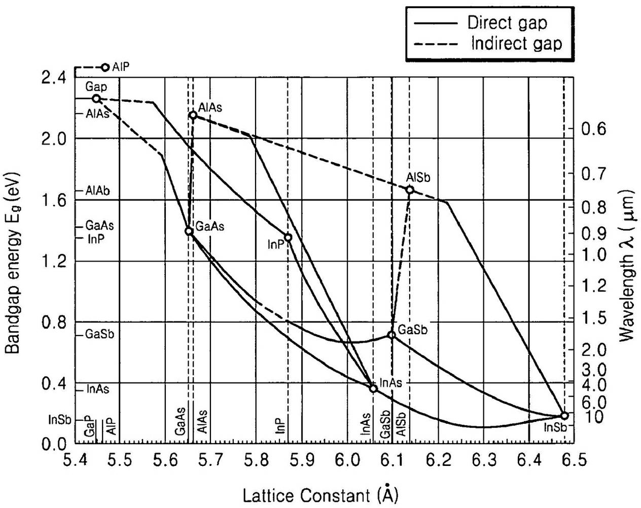
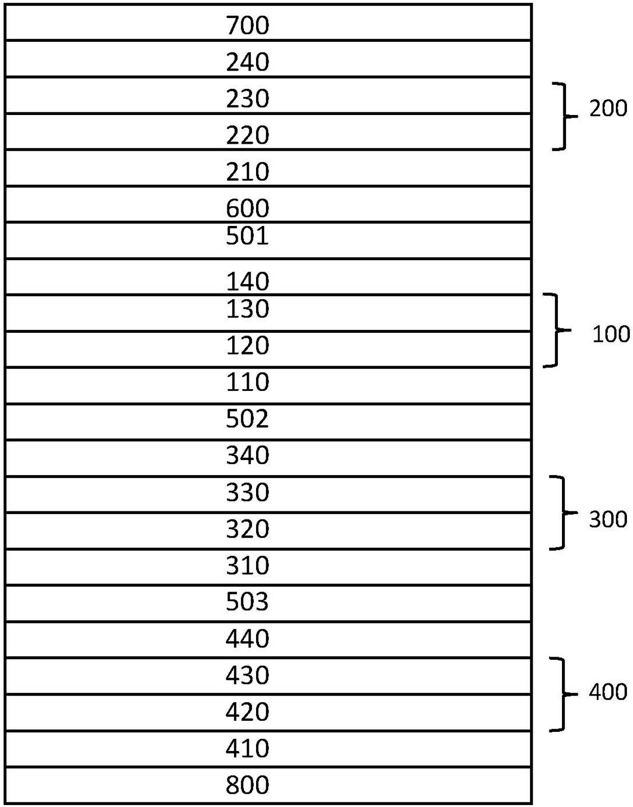
[0042] Such as figure 1 As shown, the structure of a high-efficiency four-junction solar cell includes a first sub-cell 100, a second sub-cell 200, a third sub-cell 300, and a fourth sub-cell 400, and tunnel junctions 501 and 502 are used between each junction cell. , 503 connection. Wherein, the first sub-cell 100 uses the growth substrate 001 itself as the base region 120, and implants n-type ions into the front surface of the p-type substrate to form the emitter region 130, thereby forming the first sub-cell. The arrangement order of the four-junction sub-battery from bottom to top is: the fourth sub-battery, the third sub-battery, the first sub-battery, and the second sub-battery.

[0043] The first sub-cell 100 uses the growth substrate 001 itself as the base region 120, implants n-type ions into the front of the p-type substrate to form the emitter region 130, and constitutes the first sub-cell with a band gap of 1.3-1.5 eV.

[0044] The growth substrate 001 is polishe...

Embodiment 2

[0056] This embodiment is a manufacturing process of a high-power concentrating multi-junction solar cell described in Example 1, which includes the formation process of the sub-cells 100, 200, 300, 400 and layers between the sub-cells.

[0057] The lattice constant and electrical properties in the semiconductor structure are controlled according to appropriate growth temperature and time and by using appropriate chemical compositions and dopants. Vapor deposition methods such as MOCVD and MBE can be used, but MOCVD is preferred as the growth technique of the present invention.

[0058] Concrete preparation process comprises the following steps:

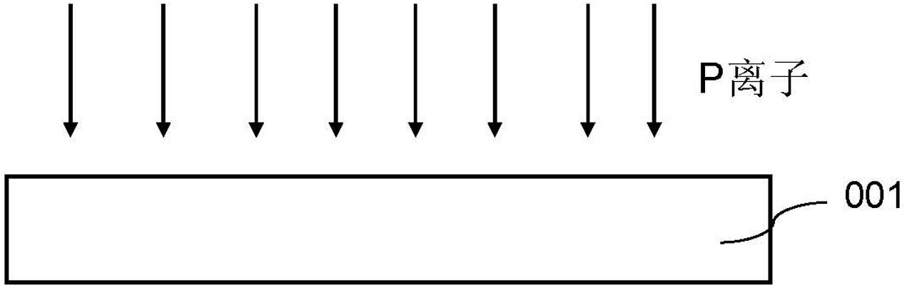
[0059] In the first step, a double-sided polished substrate 001 is provided. In this embodiment, a double-sided polished InP substrate with a p-type thickness of 200 microns is selected, and its doping concentration is 2×10 17 cm -3 ~5×10 17 cm -3 .

[0060] In the next step, the first sub-cell 100 is formed, the bandgap of whi...


PUM


Abstract

The invention discloses a high-efficient four solar cell and a manufacturing method thereof. The method is characterized by: providing a double-sided polishing substrate, which is used for growing an extension of a semiconductor; forming a first sub-cell on a front side of the substrate so that the first sub-cell possesses a first band gap; forming a gradient buffer layer above the first sub-cell so that the gradient buffer layer possesses a second band gap which is greater than the first band gap; forming a second sub-cell above the gradient buffer layer so that the second sub-cell possesses a third band gap which is greater than the second band gap; forming a high doping cap layer above the second sub-cell; forming a third sub-cell on a back side of the substrate, wherein the third sub-cell grows at an inversed direction and possesses a fourth band gap which is less than the first band gap; forming a fourth sub-cell under the third sub-cell, wherein the fourth sub-cell grows at an inversed direction and possesses a fifth band gap which is less than the fourth band gap; extending to form a back contact layer under the fourth sub-cell and acquiring the needed solar cell. By using the method of the invention, the high-efficient four solar cell with current matching and a wide spectrum absorption scope can be manufactured.

Description

technical field [0001] The invention relates to a high-efficiency four-junction solar cell and a preparation method thereof, belonging to the technical field of semiconductor materials. Background technique [0002] In the 21st century, the world's population is increasing rapidly, environmental pollution is serious, energy sources are depleted and the ecological environment is deteriorating, which makes human beings have a greater demand for energy, especially the development and utilization of clean new energy. Since the sun is an inexhaustible and inexhaustible energy source, the study of the utilization of solar energy has always been one of the major contemporary issues. Solar cells have the advantages of long life, high efficiency, reliable performance, low cost and no pollution. Almost all space equipment and devices use solar cells. III-V compound semiconductor solar cells have attracted much attention due to their high photoelectric conversion efficiency. Among th...

Claims


Application Information

Patent Timeline
Patent Type & Authority Applications(China)
IPC IPC(8): H01L31/18H01L31/0687H01L31/0693
CPCH01L31/06875Y02E10/544Y02P70/50
Inventor 毕京锋林桂江吴志浩刘建庆王良均丁杰梁兆煊林志东
Owner XIAMEN SANAN OPTOELECTRONICS TECH CO LTD
Why Eureka
Try Eureka