Manufacturing method of flat-type avalanche diode detector used for detecting single photon

An avalanche diode, single-photon detection technology, applied in sustainable manufacturing/processing, semiconductor devices, climate sustainability, etc., can solve problems such as breakdown, affecting detector performance, etc.

Inactive Publication Date: 2012-04-11
INST OF SEMICONDUCTORS - CHINESE ACAD OF SCI
View PDF4 Cites 22 Cited by
  • Summary
  • Abstract
  • Description
  • Claims
  • Application Information

AI Technical Summary

Problems solved by technology

However, due to structural factors, the planar APD is easy to break down early at the edge, which affects the performance of the detector.

Method used


Image

  • Manufacturing method of flat-type avalanche diode detector used for detecting single photon
  • Manufacturing method of flat-type avalanche diode detector used for detecting single photon
  • Manufacturing method of flat-type avalanche diode detector used for detecting single photon

Examples


Embodiment Construction

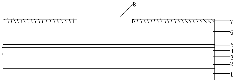
[0029] see Figure 1 to Figure 11 As shown, the present invention provides a method for manufacturing a planar avalanche diode detector that can be used for single photon detection, comprising the following steps:

[0030] Step 1: growing an InP buffer layer 2, an InGaAs absorption layer 3, an InGaAsP graded layer 4, an N-type InP charge layer 5 and an InP cap layer 6 sequentially on an N-type InP substrate 1;

[0031] Step 2: grow on the InP cap layer 6 with a thickness of SiO 2 protective layer 7;

[0032] Step 3: On SiO 2 A circular window 8 is photoetched in the middle of the protective layer 7, and the etching depth reaches the surface of the InP cap layer 6;

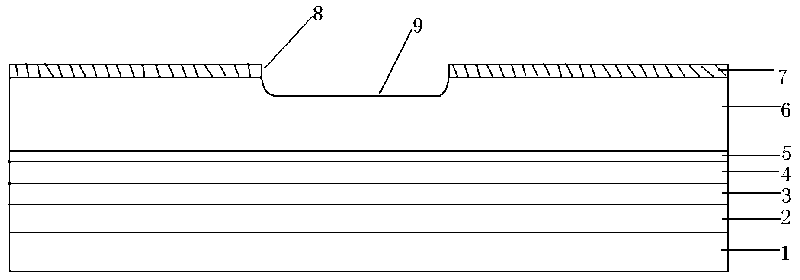
[0033] Step 4: Corrode the InP cap layer 6 in the circular window 8 by wet etching to form a circular pit 9, and the composition of the wet etching solution is Br 2 :HBr:H 2 O=1:25:80;

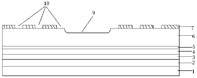
[0034] Step 5: SiO Around Circular Window 8 2 The window 10 of the protection ring is engraved on the protection layer 7...


PUM


Abstract

The invention relates to a manufacturing method of a flat-type avalanche diode detector used for detecting a single photon. The manufacturing method comprises the following steps: sequentially growing an InP buffer layer, an InGaAs absorbing layer, an InGaAsP gradient layer, an N-type InP charge layer and an InP cap layer on an N-type InP substrate; growing an SiO2 protective layer on the InP caplayer; photoengraving a round window at the middle of the SiO2 protective layer; eroding the InP cap layer in the round window through wet-method erosion, thereby forming a round hole; carving a protection ring window on the SiO2 protective layer around the round window; removing surplus SiO2 protective layer by utilizing an HF (hydrogen fluoride) solution in the protection ring window through a diffusion process; regrowing the InP cap layer an SiO2 layer, and caving an electrode window at the periphery of the round hole; forming a top ring electrode on the electrode window through an electron beam evaporation and desquamation process, and preparing a metal electrode at the periphery and one side of the ring electrode; and forming a back electrode at the back of the N-type InP substrate through electron beam evaporation, and preparing a SiNx antireflection layer at the surface of the InP cap layer in the round hole, thereby finishing the manufacture of the avalanche diode detector.

Description

technical field [0001] The invention belongs to the field of semiconductor devices, and specifically refers to a method for manufacturing a planar avalanche diode detector with double floating protection rings. Background technique [0002] In recent years, due to the rapid development of biophotonics, medical imaging, quantum communication, and encryption systems, the demand for photodetectors capable of single-photon detection has been increasing. Only by realizing the detection of weak signals or even single-photon sources can the fields mentioned above be promoted. booming. Among them, the avalanche diode detector (APD), as one of the main types that can be used for single photon detection, has been widely used in traditional optical fiber communication and other fields. Compared with PIN detectors, APD has the characteristics of its own internal gain, and does not need an external amplifier to amplify the detection signal, showing better performance than PIN. On this ...

Claims


Application Information

Patent Timeline
Patent Type & Authority Applications(China)
IPC IPC(8): H01L31/18H01L31/107H01L31/0352H01L31/0224
CPCY02P70/50
Inventor 杨怀伟李彬韩勤
Owner INST OF SEMICONDUCTORS - CHINESE ACAD OF SCI
Why Eureka
Try Eureka