

Preparation method of light absorption layer of Cu-In-Ga-Se (CIGS) film solar cell
A technology for solar cells and light-absorbing layers, which is applied in the field of solar cells and can solve problems such as the inability to accurately realize the theoretically designed energy band structure
- Summary
- Abstract
- Description
- Claims
- Application Information
AI Technical Summary
Problems solved by technology
Method used
Image

Examples
preparation example Construction
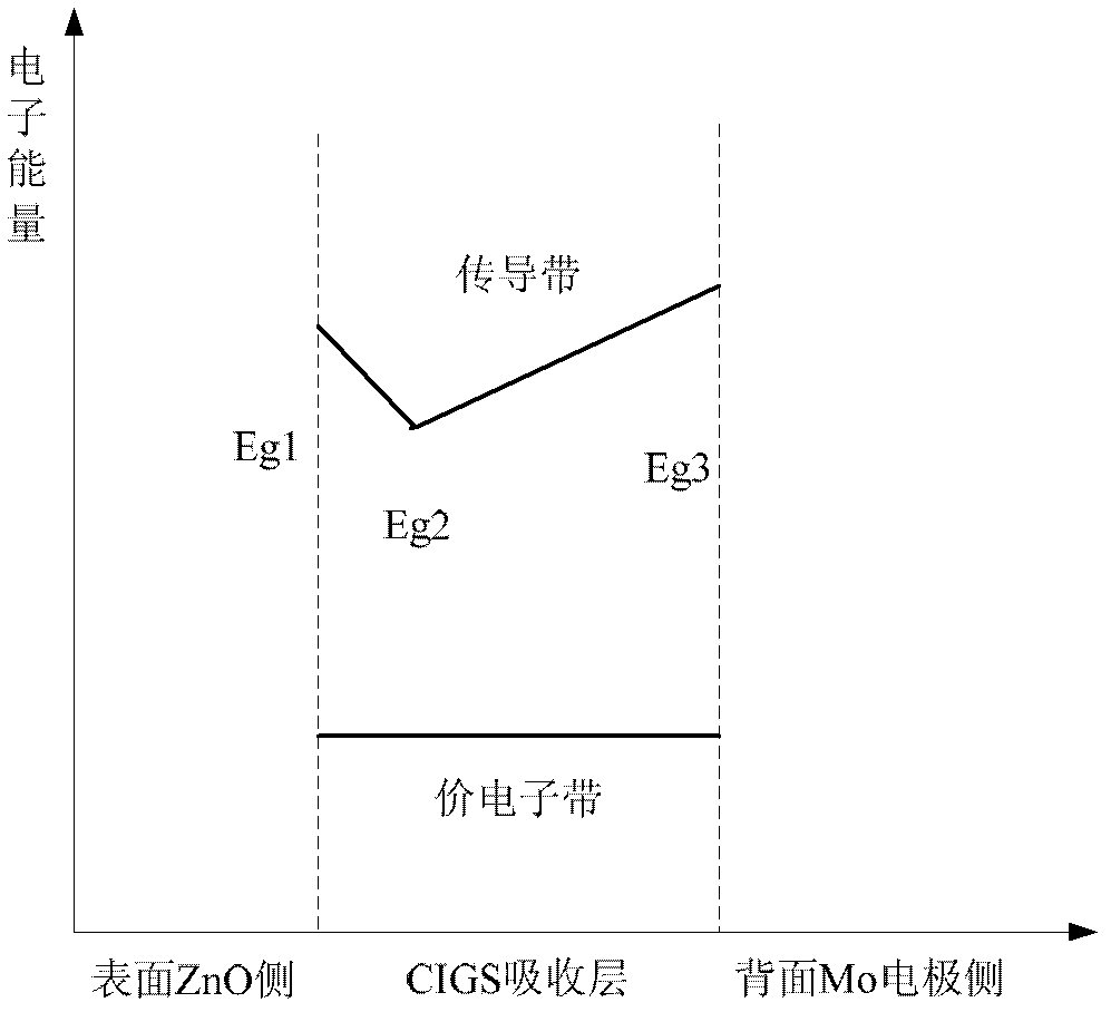
[0061] The preparation method of the above-mentioned light-absorbing layer, by controlling the evaporation of Cu to control the interaction and diffusion of various elements deposited on the substrate, realizes the final optimized V-shaped gradient bandgap structure, and controls Ga to reach the lowest concentration position in the film.
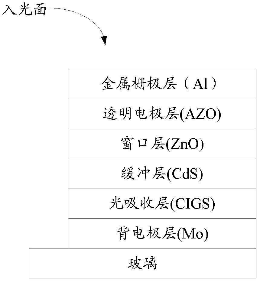
[0062] During the evaporative deposition process, the temperature of the substrate has a certain influence on the quality of the CIGS thin film. In this embodiment, when the temperature of the substrate is maintained at 450°C to 600°C, it is conducive to the formation of larger CIGS crystal particles, so that the surface of the light absorption layer is relatively smooth, and has a good relationship with the molybdenum back electrode layer. Adhesion, and the combination with the CdS buffer layer is also good.
[0063] The second evaporation process consists of two stages:
[0064] In the first stage, the temperature of the substrate is con...
Embodiment 1
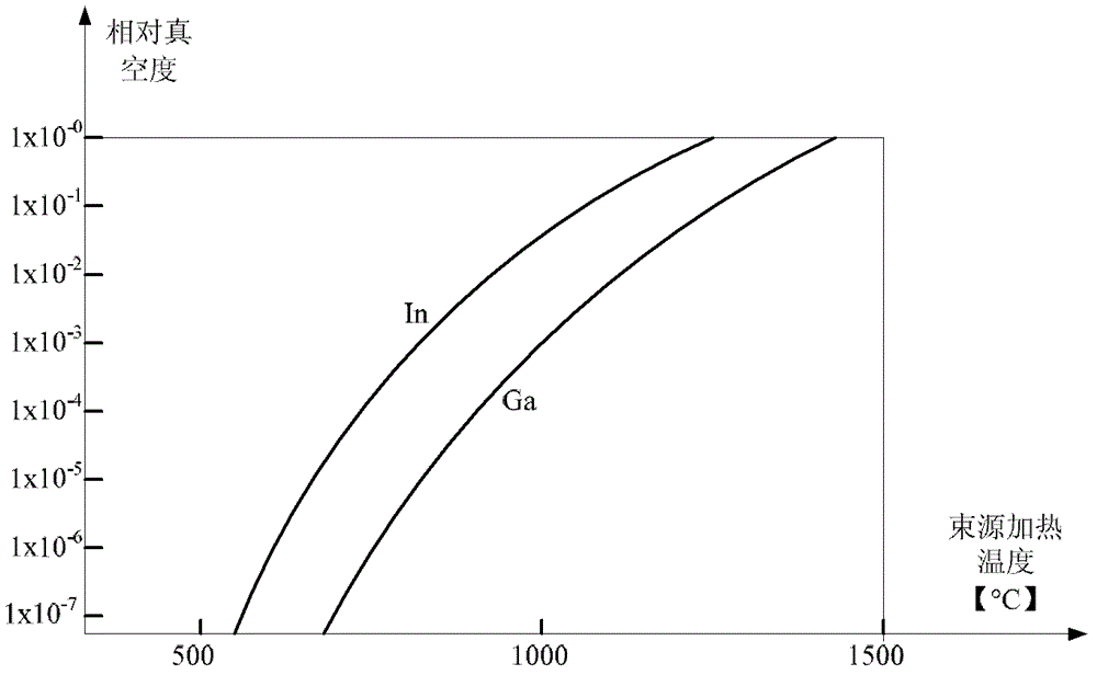
[0081] In the first stage, soda-lime glass coated with a Mo layer on the surface is provided as a substrate, and the temperature of the substrate is kept constant and kept at 250°C. The evaporation temperature of indium is 900°C and the temperature is uniformly increased by 50°C in the first stage. Gallium The evaporation temperature is 1000°C and the temperature is uniformly lowered by 40°C in the first stage, and the evaporation temperature of selenium is controlled to remain unchanged and kept at 250°C; the evaporation time of the first stage is 15min, and the first stage is formed on the Mo layer after the first stage. light absorbing layer.
[0082] The second stage: Stop evaporating indium and gallium, increase the substrate temperature to 500°C and keep it constant, keep the evaporation temperature of selenium the same as the first stage, control the evaporation temperature of copper and keep it at 1400°C; the second stage The evaporation time of the stage is about 20mi...
Embodiment 2
[0085] In the first stage, the soda-lime glass coated with Mo on the surface is provided as the substrate, the temperature of the substrate is kept constant and kept at 500°C, the evaporation temperature of indium is 900°C and the temperature is uniformly increased by 50°C in the first stage, and the temperature of the gallium is The evaporation temperature is 1000°C and the temperature is uniformly lowered by 40°C in the first stage, the evaporation temperature of selenium is controlled and kept at 250°C, the evaporation temperature of copper is kept constant and kept at 1400°C; the evaporation time of the first stage is 10min , after the end of the first stage, a light absorbing layer I is formed on the Mo layer.
[0086] The second stage: maintain the same substrate temperature as the first stage, maintain the same evaporation temperature of selenium as the first stage, maintain the same evaporation temperature of copper as the first stage, and control the initial evaporatio...
PUM
 Abstract
Description
Claims
Application Information