

Sputtering chamber, pre-cleaning chamber and plasma processing equipment
一种溅射腔、预清洗的技术,应用在溅射镀覆、离子注入镀覆、金属材料涂层工艺等方向,达到提高利用率、提高质量、降低加工成本的效果
- Summary
- Abstract
- Description
- Claims
- Application Information
AI Technical Summary
Problems solved by technology
Method used
Image

Examples
Embodiment 1
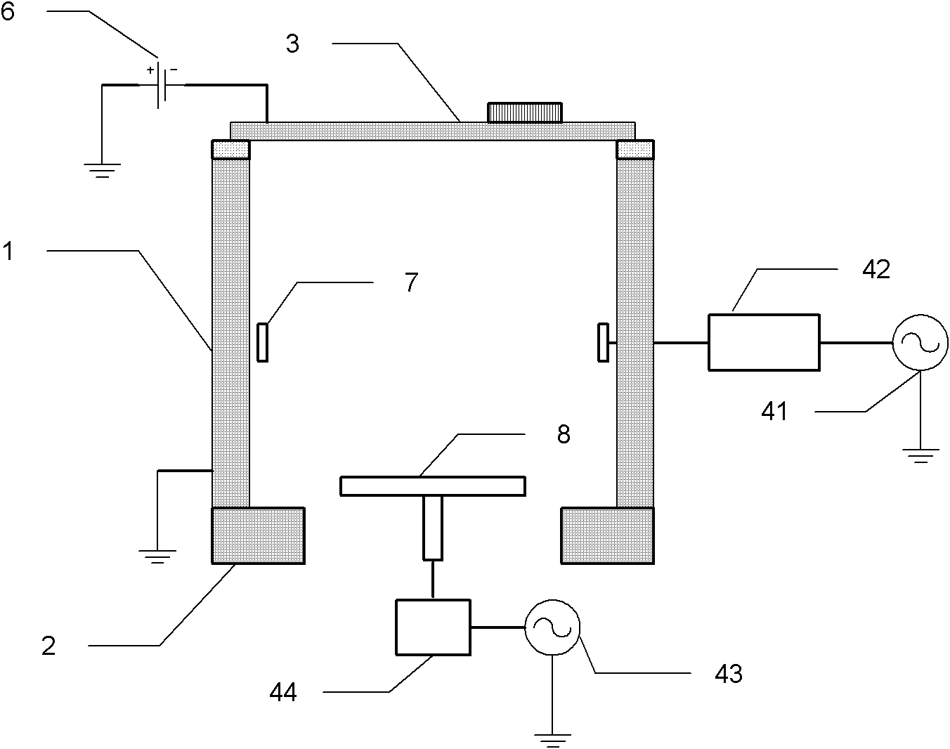
[0063] Figure 4 It is a schematic structural diagram of a sputtering chamber provided by the present invention. Such as Figure 4 As shown, the sputtering chamber includes a cavity 20 , a target 25 , an electrostatic chuck 29 and an induction coil 13 . The cavity 20 is fixed on the upper surface of the bottom wall 2 , and a target 25 is arranged on the top of the cavity 20 . The target 25, the chamber body 20 and the bottom wall 2 constitute the sputtering chamber of the plasma processing device.
[0064] The cavity 20 includes a stacked insulator cavity 21 and a first conductive sub-cavity 22, wherein the first conductive sub-cavity 22 is made of a conductive material (such as stainless steel and aluminum) and grounded, which serves as a link between the radio frequency and the DC circuit. The ground terminal is used to ensure normal plasma ignition and maintenance. The insulator cavity 21 is made of insulating material (such as ceramic or quartz).
[0065] The target 2...
Embodiment 2
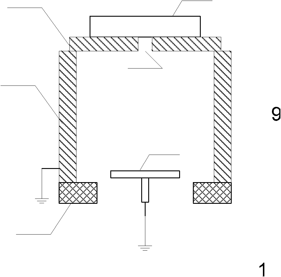
[0088] Figure 9 A schematic structural diagram of the pre-cleaning chamber provided in Embodiment 2 of the present invention. Such as Figure 9 As shown, the pre-cleaning chamber includes a chamber body 20 , a top cover 35 , an electrostatic chuck 29 and an induction coil 13 . The cavity 20 is fixed on the upper surface of the bottom wall 2 , and the top cover 35 is arranged on the top of the cavity 20 . The top cover 35, the chamber body 20 and the bottom wall 2 form a pre-cleaning chamber.
[0089] The cavity 20 includes a cylindrical second conductive sub-cavity 23 , an insulator cavity 21 and a first conductive sub-cavity 22 stacked sequentially from top to bottom, and the second conductive sub-cavity 23 and the first conductive sub-cavity The body 22 is grounded to serve as the ground terminal of the radio frequency and DC circuits, and is used to ensure normal plasma ignition and maintenance.
[0090] The inductance coil 13 is arranged outside the insulator cavity 2...
Embodiment 3
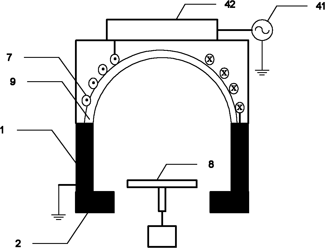
[0096] Figure 10 A schematic structural diagram of the pre-cleaning chamber provided in Embodiment 3 of the present invention. see Figure 10 , the pre-cleaning chamber includes a cavity 20 , a target 39 , an electrostatic chuck 29 and an induction coil 13 . The cavity 20 is fixed on the upper surface of the bottom wall 2 , and the top cover 35 is arranged on the top of the cavity 20 . The top cover 35, the chamber body 20 and the bottom wall 2 constitute a sputtering chamber.
[0097] The cavity 20 includes a cylindrical second conductive sub-cavity 23 , an insulator cavity 21 and a first conductive sub-cavity 22 stacked sequentially from top to bottom, and the second conductive sub-cavity 23 and the first conductive sub-cavity The body 22 is grounded as the ground terminal of the radio frequency and DC circuits to ensure normal plasma ignition and maintain the plasma.
[0098] The inductance coil 13 is arranged outside the insulator cavity 21 and connected to the first ...
PUM
| Property | Measurement | Unit |
|---|---|---|
| diameter | aaaaa | aaaaa |
Abstract
Description
Claims
Application Information