Self-recovery stop type protection circuit for low-voltage and high-power safety barrier
A technology for protecting circuits and power switching circuits, applied in the direction of protection against overcurrent, etc., can solve problems such as monitoring and monitoring systems that are not widely used, hidden safety hazards, etc., and achieve novel and reasonable design, small power loss, and large output power Effect
- Summary
- Abstract
- Description
- Claims
- Application Information
AI Technical Summary
Problems solved by technology
Method used
Image
Examples
Embodiment 1
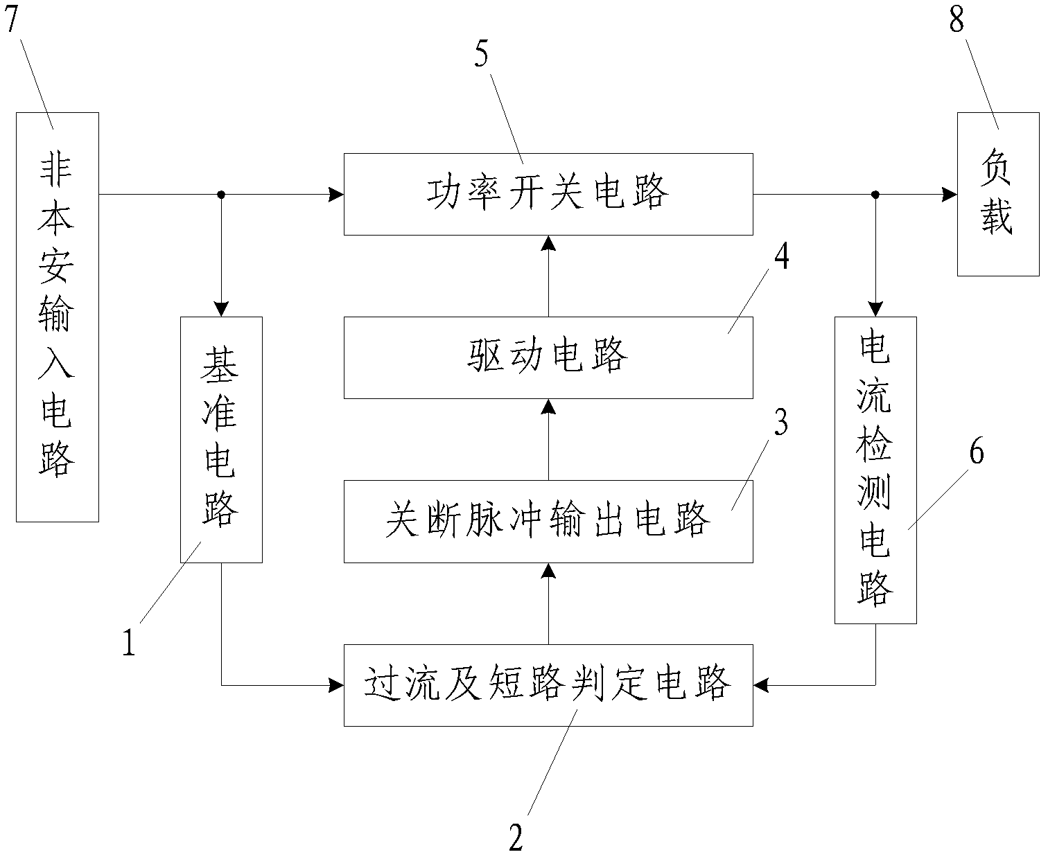
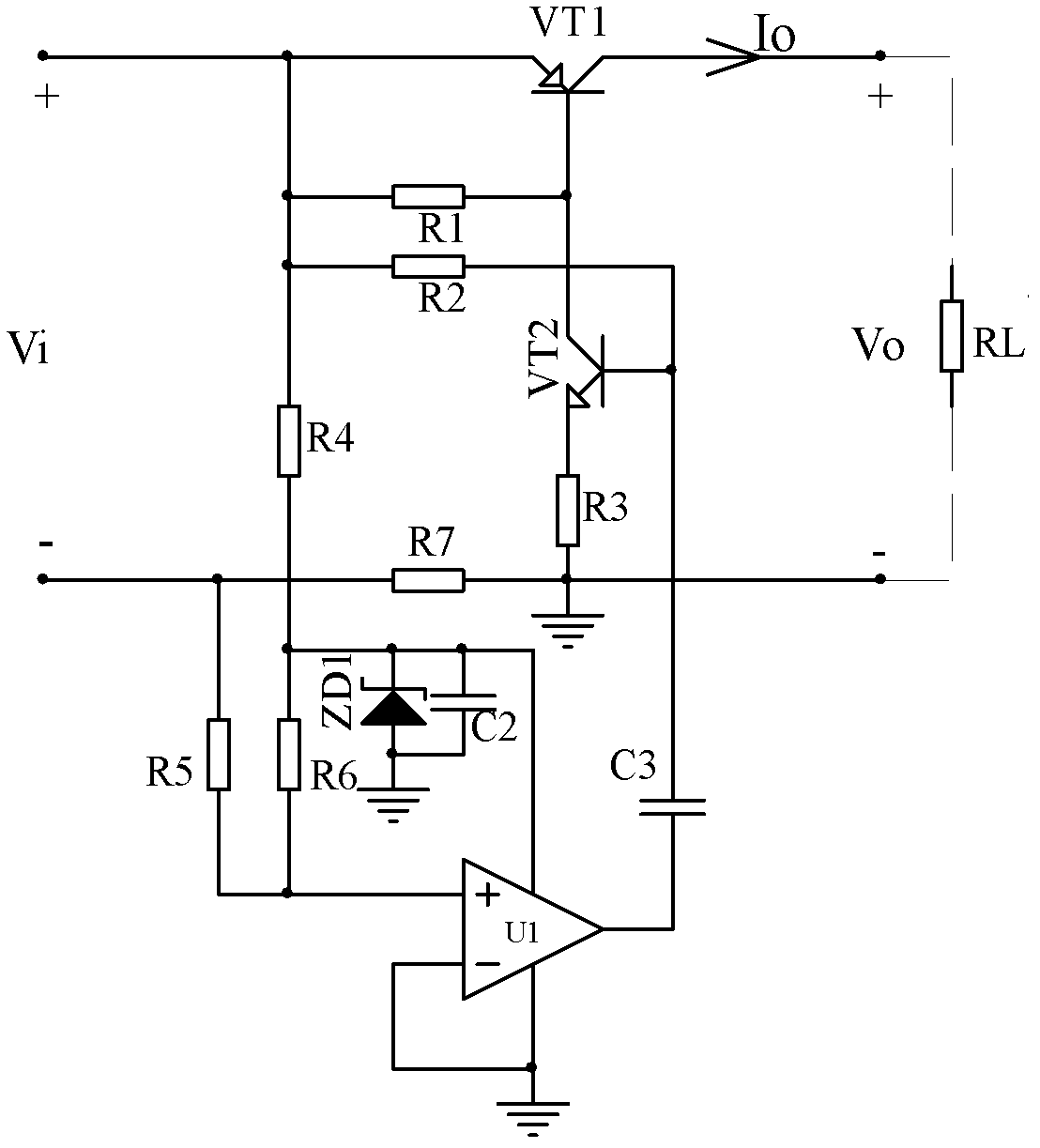
[0034] like figure 1 As shown, the present invention is connected between the non-intrinsically safe input circuit 7 and the load 8, including the power switch circuit 5 connected between the non-intrinsically safe input circuit 7 and the load 8 and used to control the opening or closing of the circuit, and the power switch The circuit 5 is connected to the current detection circuit 6 for real-time detection of the current in the circuit, the overcurrent and short circuit judgment circuit 2 is connected to the current detection circuit 6 and used to determine whether there is an overcurrent or short circuit phenomenon, and the overcurrent and short circuit A shutdown pulse output circuit 3 connected to the judgment circuit 2 and used to output a shutdown pulse signal when an overcurrent or short circuit occurs, and a drive connected to the shutdown pulse output circuit 3 and used to control the power switch circuit 5 to be turned off or turned on Circuit 4, the input terminal ...
Embodiment 2
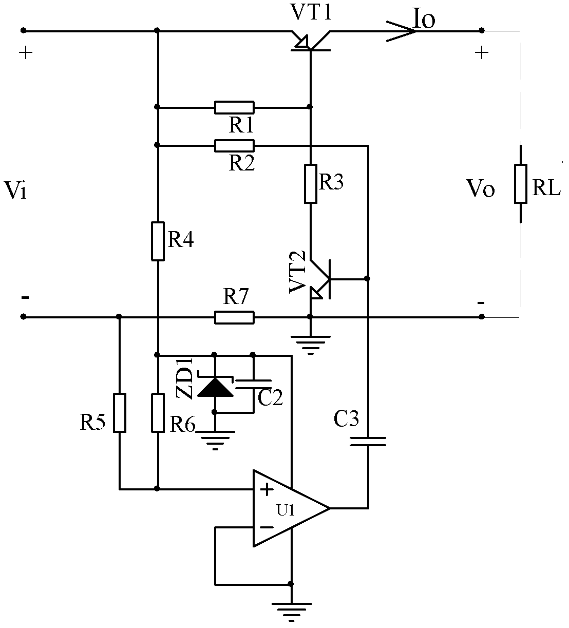
[0042] combine image 3 The difference between this embodiment and Embodiment 1 is that the emitter of the NPN transistor VT2 is grounded, the collector of the NPN transistor VT2 is connected to one end of the resistor R3, and the other end of the resistor R3 is the drive circuit 4 outputs. The rest of the circuit structure is the same as that of Embodiment 1.
Embodiment 3
[0044] combine Figure 4 The difference between this embodiment and Embodiment 1 is that the power switch circuit 5 includes a resistor R1 and an enhancement-mode PMOS transistor VT3, and one end of the resistor R1 and the source of the enhancement-mode PMOS transistor VT3 are both connected to the non-intrinsically safe input circuit. 7 is connected to the positive output end of the resistor R1, the other end of the resistor R1 is connected to the gate of the enhanced PMOS transistor VT3 and is connected to the output end of the drive circuit 4, and the drain of the enhanced PMOS transistor VT3 is a power switch circuit. The positive output terminal of 5 is connected to the positive terminal of load 8. The rest of the circuit structure is the same as that of Embodiment 1.
PUM
 Abstract
Description
Claims
Application Information


