SOI structure with reinforced anti-irradiation performance and manufacturing method thereof

A radiation-resistant and radiation-resistant technology, which is applied in semiconductor/solid-state device manufacturing, electrical components, circuits, etc., can solve problems such as injection damage of top-layer materials, affecting the effect of material anti-radiation reinforcement, etc., to achieve the reduction of the number of holes, The effect of improving the radiation resistance performance

Active Publication Date: 2012-05-02
BEIJING ZHONGKE XINWEITE SCI & TECH DEV
View PDF2 Cites 11 Cited by
  • Summary
  • Abstract
  • Description
  • Claims
  • Application Information

AI Technical Summary

Problems solved by technology

[0005] However, while implanting ions into the buried oxide layer, it will inevitably cause some implantation damage to the top layer material; in addition, while ion implantation can effectively improve the radiation resistance of the buried oxide layer, it will definitely affect the buried oxide layer. The internal microstructure of the material is macroscopically manifested as a change in the electrical properties of the buried oxide layer, and such changes may in turn affect the radiation-resistant strengthening effect of ion implantation on the material.

Method used


Image

  • SOI structure with reinforced anti-irradiation performance and manufacturing method thereof
  • SOI structure with reinforced anti-irradiation performance and manufacturing method thereof
  • SOI structure with reinforced anti-irradiation performance and manufacturing method thereof

Examples


Embodiment Construction

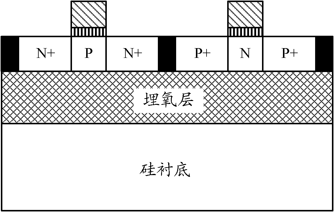
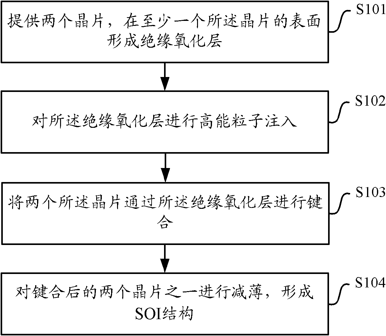
[0021] Embodiments of the invention are described in detail below, examples of which are illustrated in the accompanying drawings. The embodiments described below by referring to the figures are exemplary only for explaining the present invention and should not be construed as limiting the present invention.

[0022] The following disclosure provides many different embodiments or examples for implementing different structures of the present invention. To simplify the disclosure of the present invention, components and arrangements of specific examples are described below. Of course, they are only examples and are not intended to limit the invention. Furthermore, the present invention may repeat reference numerals and / or letters in different instances. This repetition is for the purpose of simplicity and clarity and does not in itself indicate a relationship between the various embodiments and / or arrangements discussed. In addition, various specific process and material exam...


PUM


Abstract

The invention provides an SOI (Silicon-On-Insulator) structure with reinforced anti-irradiation performance and a manufacturing method thereof. The manufacturing method of the SOI structure with reinforced anti-irradiation performance comprises the following steps: providing two wafers, and forming an insulation oxide layer on a surface of at least one wafer; carrying out injection of an irradiation proton, an irradiation neutron and the like on the insulation oxide layer, and introducing displacement damage in the insulation oxide layer; carrying out bonding of the two wafers through the insulation oxide layer; thinning one of the two wafers after bonding to form an SOI structure. In a process of utilizing bonding technology to prepare an SOI, through a method of injecting the proton, the neutron and the like into a buried oxide layer and introducing the displacement damage to form a composite center, anti-irradiation performance of an SOI device is raised, simultaneously, damage of a top silicon layer is avoided, and the performance of the device is not influenced.

Description

technical field [0001] The invention relates to semiconductor manufacturing technology, in particular to a reinforced SOI structure with anti-radiation performance and a manufacturing method thereof. Background technique [0002] Compared with other semiconductor device technologies, silicon-on-insulator (Silicon-On-Insulator, SOI) technology is a full dielectric isolation technology. A typical SOI CMOS structure such as figure 1 As shown, there is a dielectric layer-buried oxide layer between the top silicon film and the substrate to isolate the active region of the device from the substrate. Because the buried oxide layer achieves good isolation, SOI devices have incomparable advantages in terms of device radiation resistance performance, which is also the motivation for the initial development of SOI technology. [0003] Although the SOI device achieves good isolation due to the existence of the buried oxide layer, the active area of ​​the device is small, has lower lea...

Claims


Application Information

Patent Timeline
Patent Type & Authority Applications(China)
IPC IPC(8): H01L21/762
Inventor 吕荫学毕津顺罗家俊韩郑生叶甜春
Owner BEIJING ZHONGKE XINWEITE SCI & TECH DEV
Why Eureka
Try Eureka