

Dense-pitch small-pad copper-wire bonded single intelligent card (IC) chip packing piece and preparation method thereof
A chip package and small pad technology, which is applied in semiconductor/solid-state device manufacturing, electrical components, electric solid-state devices, etc., can solve the problems of short circuit of adjacent solder joints, damage of adjacent bonding wires, etc., and achieve bonding strength Excellent, save the cost of welding wire, improve the effect of product quality
- Summary
- Abstract
- Description
- Claims
- Application Information
AI Technical Summary
Problems solved by technology
Method used
Image

Examples
Embodiment 1
[0035] The process flow of preparing packages is thinning, scribing, core bonding, pressure welding, plastic sealing, post-curing, rib cutting, electroplating, printing, forming separation and packaging, in which other processes except core core and pressure welding processes are adopted The conventional method of related packaging forms, the process of chipping and bonding operation is as follows:
[0036] 1. Thinning and scribing
[0037]Thinning the wafer to 280μm and dicing by adopting general packaging thinning equipment and process;
[0038] 2. Core loading
[0039] Using the eSOP, eMSOP, eTSSOP, e / TLQFP, QFN, DFN lead frame with the exposed carrier, fix the 1 thinned and diced IC chip 3 on the above lead frame carrier 1 with adhesive 2, the core loading equipment and process Production of conventional products in the same packaging form;
[0040] 3. Baking
[0041] Use N 2 The anti-separation layer baking technology with an air flow rate of 25ml / min bakes the lead ...
Embodiment 2
[0052] 1. Thinning and scribing
[0053] Thinning the wafer to 300μm and dicing by adopting general packaging thinning equipment and process;
[0054] 2. Core loading
[0055] Using eSOP, eMSOP, eTSSOP, e / TLQFP, QFN, DFN lead frame with exposed carrier, fix 1 IC chip 3 that has been thinned and diced on the above lead frame carrier 1 with conductive glue, and the chipping equipment and process are related to the same Production of conventional products in package form;
[0056] 3. Baking
[0057] Use N 2 The anti-separation layer baking technology with an air flow rate of 30ml / min bakes the lead frame carrier for 3 hours at a baking temperature of 150°C;
[0058] 4. Pressure welding
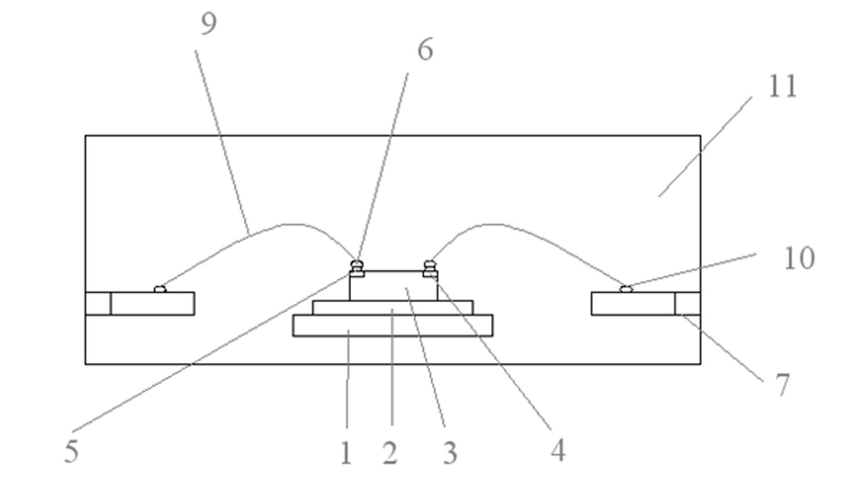
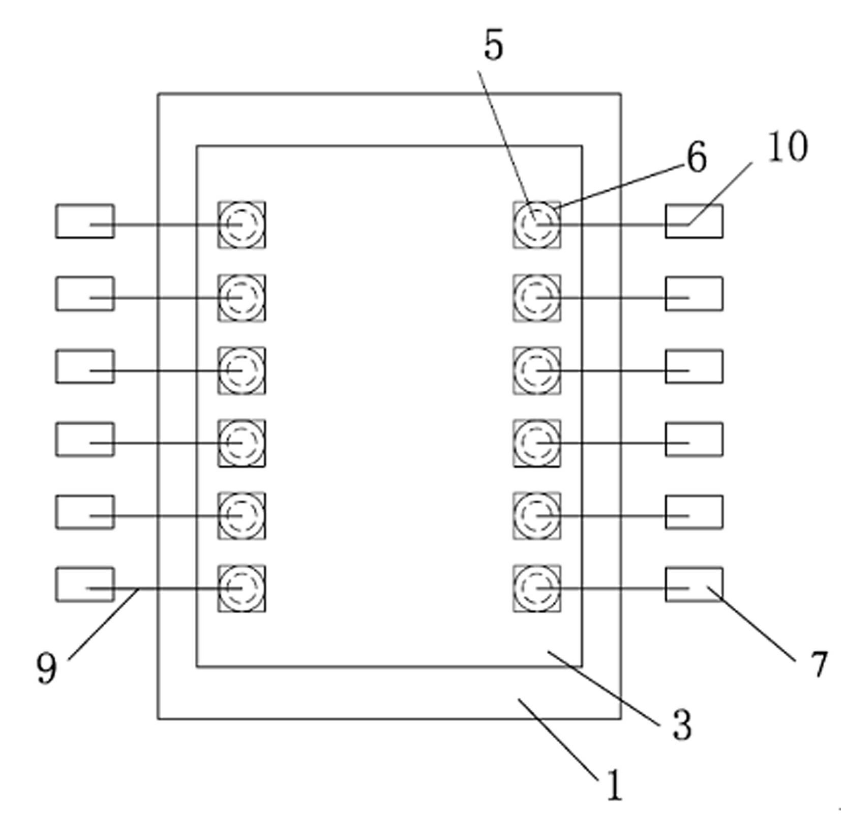
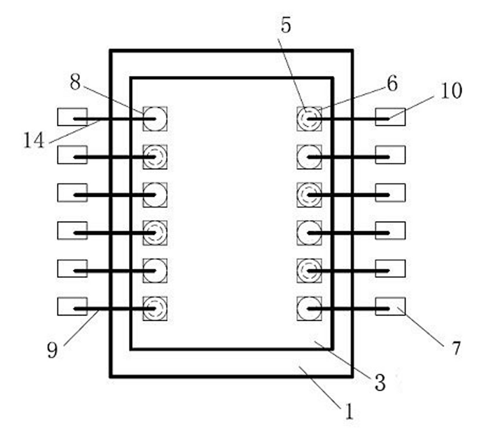
[0059] (1) Two rows of pad groups are arranged in parallel on the upper surface of the IC chip 3 installed in step 1, and the two rows of pad groups are respectively composed of the same or different numbers of pads 4, and each pad in the two rows 4 are not in contact with each other, the p...
Embodiment 3
[0070] 1. Thinning and scribing
[0071] Use relevant packaging forms to thin general-purpose equipment and processes, and wafers are thinned by 250 μm and diced;
[0072] 2. Core loading
[0073] The upper core adopts SOP, SSOP, MSOP, TSSOP, QFPL, QFP, QFN, DFN lead frame with no exposed carrier, and the IC chip 3 that has been thinned to 250 μm and diced is fixed on the above lead frame carrier 1 with insulating glue , the chip-on equipment and process are the same as those of conventional products in related packaging forms;
[0074] 3. Pressure welding
[0075] (1) On the upper surface of the IC chip 3 installed in step 1, two rows of pad groups are arranged in parallel, and the two rows of pad groups are respectively composed of the same number of pads 4, and the gap between each pad 4 in the two rows of pad groups is Not in contact with each other, the pads 4 in one row of pad groups correspond to the pads 4 in the other row of pad groups, such as figure 1 As shown, ...
PUM
| Property | Measurement | Unit |
|---|---|---|
| Pitch | aaaaa | aaaaa |
| Diameter | aaaaa | aaaaa |
| Diameter | aaaaa | aaaaa |
Abstract
Description
Claims
Application Information