Process for increasing capacitance density of integrated circuit
A process and capacitor technology, applied in the field of semiconductor integrated circuit manufacturing, can solve the problems of reduced dielectric layer thickness, reduced breakdown voltage, etc., and achieve the effects of good compatibility, simple process, and good self-shielding effect
- Summary
- Abstract
- Description
- Claims
- Application Information
AI Technical Summary
Problems solved by technology
Method used
Image

Examples
Embodiment Construction
[0036] The present invention will be further described below in combination with schematic diagrams and specific operation examples.
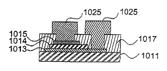
[0037] Such as figure 1 as shown, figure 1 It is a schematic diagram of a traditional MIM process, in which 1011 is a substrate material, 1013 is the first layer of doped polysilicon, 1014 is a dielectric material, a kind of oxide, 1015 is the second layer of doped polysilicon, and 1025 are respectively 1013 is an electrode connected to the first layer of doped polysilicon, 1015 is the second layer of doped polysilicon, and 1017 is a dielectric layer. This kind of capacitor is easy to cause breakdown leakage, and this kind of capacitor occupies a large area. With the continuous improvement of semiconductor integrated circuit manufacturing technology, the performance is continuously improved, and it is also accompanied by the process of device miniaturization and miniaturization. More and more advanced manufacturing processes require as many d...
PUM
 Abstract
Description
Claims
Application Information
 - R&D
- Intellectual Property
- Life Sciences
- Materials
- Tech Scout
- Unparalleled Data Quality
- Higher Quality Content
- 60% Fewer Hallucinations
Browse by: Latest US Patents, China's latest patents, Technical Efficacy Thesaurus, Application Domain, Technology Topic, Popular Technical Reports.
© 2025 PatSnap. All rights reserved.Legal|Privacy policy|Modern Slavery Act Transparency Statement|Sitemap|About US| Contact US: help@patsnap.com