Method for reducing germanium/silicon epitaxy surface defects

A silicon germanium epitaxy and silicon wafer surface technology, which is applied to chemical instruments and methods, from chemically reactive gases, crystal growth, etc., can solve the problems of epitaxial layer crystal defects, quality reduction and poor effect of germanium silicon epitaxial growth, etc.

Inactive Publication Date: 2012-05-16
SHANGHAI HUAHONG GRACE SEMICON MFG CORP
View PDF2 Cites 3 Cited by
  • Summary
  • Abstract
  • Description
  • Claims
  • Application Information

AI Technical Summary

Problems solved by technology

At this time, high-temperature hydrogen baking becomes a problem, that is, the baking temperature should not be too high; but lowering the baking temperature will reduce the baking effect, such as below 800 ° C, the effect of hydrogen baking to remove the natural oxide layer will be reduced very poor (see image 3 ), the epitaxial layer has many crystalline defects, which will lead to a decrease in the quality of the subsequent silicon germanium epitaxial growth

Method used


Image

  • Method for reducing germanium/silicon epitaxy surface defects
  • Method for reducing germanium/silicon epitaxy surface defects
  • Method for reducing germanium/silicon epitaxy surface defects

Examples


Embodiment 1

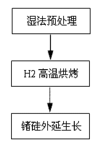
[0021] combine figure 2 Shown, in the present embodiment, the implementation process of the method of the present invention is as follows:

[0022] In the first step, the oxide layer and pollutants on the surface of the silicon wafer are removed by wet pretreatment.

[0023] In the second step, the silicon wafer is transported to the silicon germanium process chamber, and the surface of the silicon wafer is treated with HF gas under a certain temperature and pressure before the growth of silicon germanium. The function of HF gas treatment is to remove the natural oxide layer on the surface of the silicon wafer, the temperature during treatment is 100-800°C, and the pressure is 0.01-760Torr. In this embodiment, for example, the temperature is 400° C. and the pressure is 20 torr.

[0024] The third step is to adjust the process parameters and carry out epitaxial growth of silicon germanium on the surface of the silicon wafer. The parameters of germanium-silicon epitaxial gro...

Embodiment 2

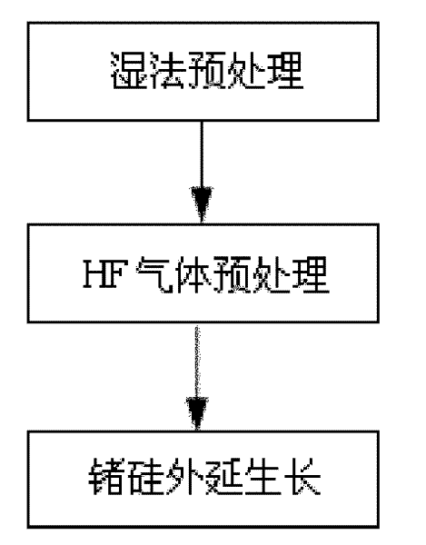
[0026] combine figure 2 Shown, the method implementation process of the present invention is as follows:

[0027] In the first step, the oxide layer and pollutants on the surface of the silicon wafer are removed by wet pretreatment;

[0028] The second step is to transfer the silicon wafer to the silicon germanium process machine, first enter the HF pretreatment chamber, and in a vacuum or inert gas state (does not react with silicon), under a certain temperature and pressure, in the silicon germanium epitaxy Before the growth, the surface of the silicon wafer is treated with HF gas, for example, the temperature is 400° C., and the pressure is 20 torr. Then the silicon wafer is transferred to the silicon germanium process chamber, and the transfer process is in a vacuum state or an inert gas state (does not react with silicon).

[0029] The third step is to adjust the process parameters and carry out epitaxial growth of silicon germanium. The parameters of silicon germaniu...


PUM


Abstract

The invention discloses a method for reducing germanium / silicon epitaxy surface defects, comprising the following steps of: Step 1, removing oxide and pollutants on the surface of silicon chip by a wet method; Step 2, processing the surface of the silicon chip by hydrofluoric acid HF gas; and Step 3, carrying out germanium / silicon epitaxy growth on the surface of the silicon chip. By the adoption of the method provided by the invention, thermal budget of a germanium / silicon technology can be reduced and the germanium / silicon epitaxy quality can be raised.

Description

technical field [0001] The invention relates to the field of semiconductor integrated circuits, in particular to a method for reducing surface defects of germanium and silicon epitaxy. Background technique [0002] The silicon epitaxial process, especially the low temperature (<1000° C.) silicon / germanium silicon (SiGe) epitaxial (Epi) process, has high requirements on the surface of the silicon wafer before growth. combine figure 1 As shown, for ordinary (high temperature) epitaxy process, the oxide layer and pollutants on the surface of the silicon wafer are usually removed by wet pretreatment, and the natural oxide film formed on the surface of the silicon wafer after wet pre-cleaning and before the growth of silicon germanium can be grown by Previous high temperature (>1000°C) hydrogen (H 2 ) is baked and burned to achieve a better surface quality, for example, if baked at 1100°C, the growth of the epitaxial layer is relatively perfect (see Figure 4 ); and then si...

Claims


Application Information

Patent Timeline
IPC IPC(8): C30B25/02H01L21/02
Inventor 刘继全
Owner SHANGHAI HUAHONG GRACE SEMICON MFG CORP
Why Eureka
Try Eureka