Nitride semiconductor light-emitting device

A technology of nitride semiconductors and light-emitting elements, applied in semiconductor devices, electrical components, circuits, etc., can solve the problems of light output reduction and absorption ratio increase of light-emitting elements, so as to prevent light output reduction, suppress heat generation, and increase current Effects of Diffusion and Light Uniformity

Active Publication Date: 2012-05-16
HUAIAN AUCKSUN OPTOELECTRONICS TECHNOLOGY CO LTD
View PDF10 Cites 5 Cited by
  • Summary
  • Abstract
  • Description
  • Claims
  • Application Information

AI Technical Summary

Problems solved by technology

[0012] In the case of providing branch electrodes in the light-emitting element as in JP 2003-524295 A and JP 2000-164930 A, it is effective for reducing the driving voltage and improving the current spreading characteristics, but as long as the area of ​​the branch electrodes becomes Larger, the light from the light-emitting layer is blocked by the branch electrodes, the ratio of absorption increases, and there is a problem that the light output of the light-emitting element decreases.

Method used


Image

  • Nitride semiconductor light-emitting device
  • Nitride semiconductor light-emitting device
  • Nitride semiconductor light-emitting device

Examples


Embodiment 1

[0044] In embodiment 1 of the present invention, make and figure 1 and figure 2 A light-emitting element similar to the light-emitting element schematically illustrated in . image 3 (A) is a schematic plan view showing the light-emitting element of the first embodiment.

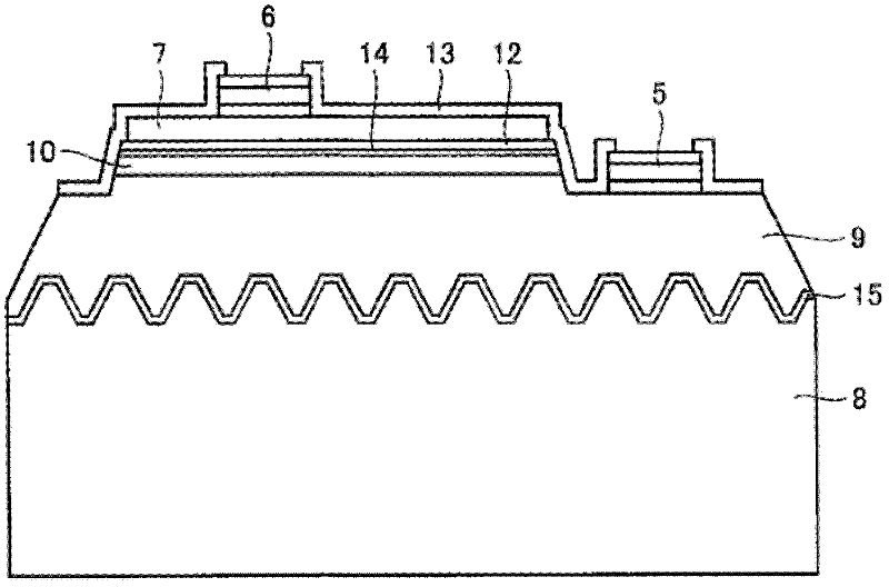
[0045] Such as figure 2 As schematically shown, in the light-emitting element of Example 1, an n-type nitride semiconductor layer 9 is deposited via an AlN buffer layer 15 on a sapphire substrate 8 having a main surface in the (0001) plane direction. The n-type semiconductor layer 9 includes: a GaN base layer with a thickness of 9 μm and a Si-doped n-type GaN contact layer with a thickness of 2 μm deposited at a substrate temperature of about 1000° C., with a carrier concentration of about 6×10 18 cm -3 .

[0046] A nitride semiconductor active layer 10 is deposited on the n-type semiconductor layer 9 . The active layer 10 has a multiple quantum well structure. On the basis of a substrate temperatur...

Embodiment 2

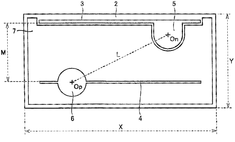
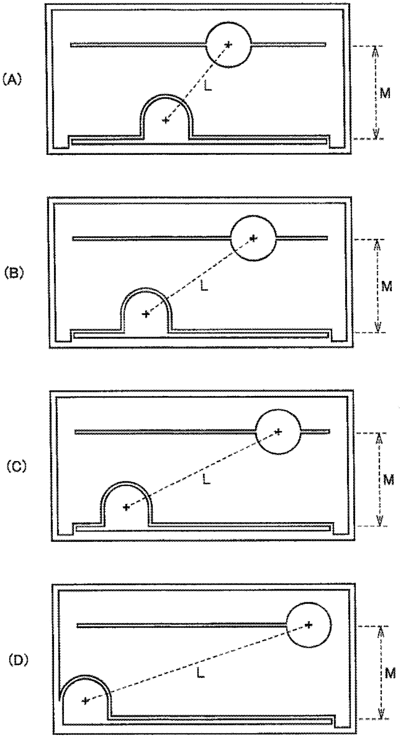
[0066] image 3 (B) is a plan view schematically showing the light-emitting element of Example 2 of the present invention. Compared with Example 1, the light-emitting element of this Example 2 is only different in the value of the ratio M / L. In Example 2, the distance M between the branch electrodes and the distance L between the centers of the p-side and n-side electrode pads The ratio M / L was reduced to 0.7. By comparison image 3 (A) and image 3 (B) just can see clearly the change of M / L value in embodiment 1 and embodiment 2.

[0067] From Figure 6 (B) and Figure 6 (C) It can be seen that in the case of driving the light-emitting element with a current of 100mA, wherein the current density>90A / cm 2 , current injection area: 1.10×10 -3 cm 2 , the light output Po (mW) and power efficiency WPE (%) of the light emitting element (M / L=0.70) of Example 2 were the highest.

Embodiment 3

[0069] image 3(C) is a plan view schematically showing a light-emitting element according to Example 3 of the present invention. Compared with the other embodiments, the light-emitting element of Example 3 is only different in the value of the ratio M / L, and the ratio M / L of the distance M between the branch electrodes to the distance L between the centers of the p-side and n-side electrode pads is further improved. Reduced to 0.5.

[0070] Figure 7 An optical photograph taken with a CCD camera (HAMAMATSU C8000-20) of the light emitting state of the light emitting element is shown. The optical photographs attached here are shown as black and white shaded photographs, but the original optical photographs are shown in red, orange, yellow, green, light blue, blue, and navy in order from areas with more light to areas with less light. A color photograph of wavelength variation. When the color photo is converted into a black and white photo, green at an intermediate wavelengt...


PUM


Abstract

A nitride semiconductor light-emitting device includes at least one n-type semiconductor layer, an active layer and at least one p-type semiconductor layer within a rectangle nitride semiconductor region on a substrate. The n-type semiconductor layer has a partial exposed area, a p-side branch electrode integral with a p-side electrode pad formed on a current diffusion layer formed on the p-type semiconductor layer, an n-side branch electrode integral with an n-side electrode pad formed on the partial exposed area of the n-type semiconductor layer, the p-side and n-side branch electrodes extend parallel to each other along two opposite sides of the semiconductor region, and conditions of 0.3<M / L<1.1 and L<Lmax are satisfied; L is the distance between centers of the p-side and n-side electrode pads, M is the distance between the p-side and n-side branch electrodes, and Lmax represents a distance between the centers of the p-side and n-side electrode pads.

Description

technical field [0001] The present invention relates to the use of nitride semiconductors (In X Al Y Ga 1-X-Y N, 0 ≤ x < 1, 0 ≤ y < 1) produced light-emitting devices, and particularly relates to nitride semiconductor light-emitting devices that can be used as high-intensity light sources such as backlights for liquid crystal display devices and general lighting. Background technique [0002] A general nitride semiconductor light-emitting element includes an n-type nitride semiconductor layer, a nitride semiconductor light-emitting layer and a p-type nitride semiconductor layer deposited sequentially on a sapphire substrate. On the p-type semiconductor layer side and the n-type semiconductor layer side, a p-side electrode pad and an n-side electrode pad for connection to an external power supply are formed, respectively. [0003] Generally, the p-type nitride semiconductor layer has higher film resistance than the n-type nitride semiconductor layer, so for the purpo...

Claims


Application Information

Patent Timeline
Patent Type & Authority Applications(China)
IPC IPC(8): H01L33/20H01L33/14H01L33/38H01L33/64
CPCH01L33/20H01L33/42H01L33/38
Inventor 翁宇峰M.布罗克利
Owner HUAIAN AUCKSUN OPTOELECTRONICS TECHNOLOGY CO LTD
Why Eureka
Try Eureka