High voltage iii-nitride semiconductor devices

A technology of nitride and nitride layer, which is applied in the direction of semiconductor devices, semiconductor/solid-state device manufacturing, electrical components, etc., and can solve problems such as current collapse

Active Publication Date: 2015-04-15
TRANSPHORM INC
View PDF11 Cites 0 Cited by
  • Summary
  • Abstract
  • Description
  • Claims
  • Application Information

AI Technical Summary

Problems solved by technology

However, defects that form deep levels in the buffer layer also diffuse into the channel layer, where they can easily trap electrons and cause current collapse

Method used


Image

  • High voltage iii-nitride semiconductor devices
  • High voltage iii-nitride semiconductor devices
  • High voltage iii-nitride semiconductor devices

Examples


Embodiment Construction

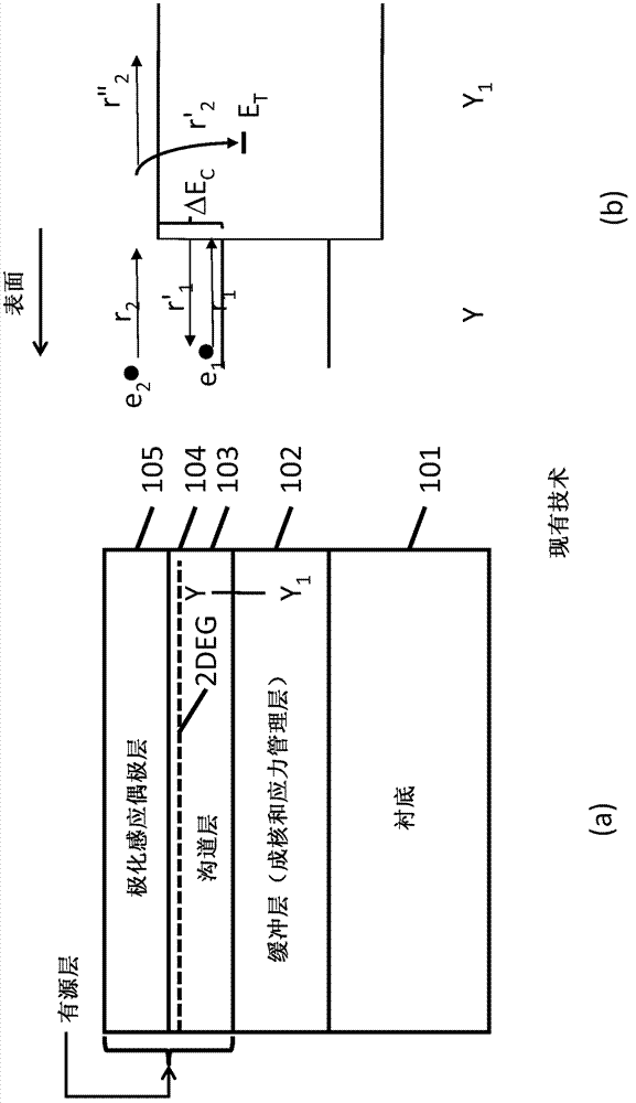
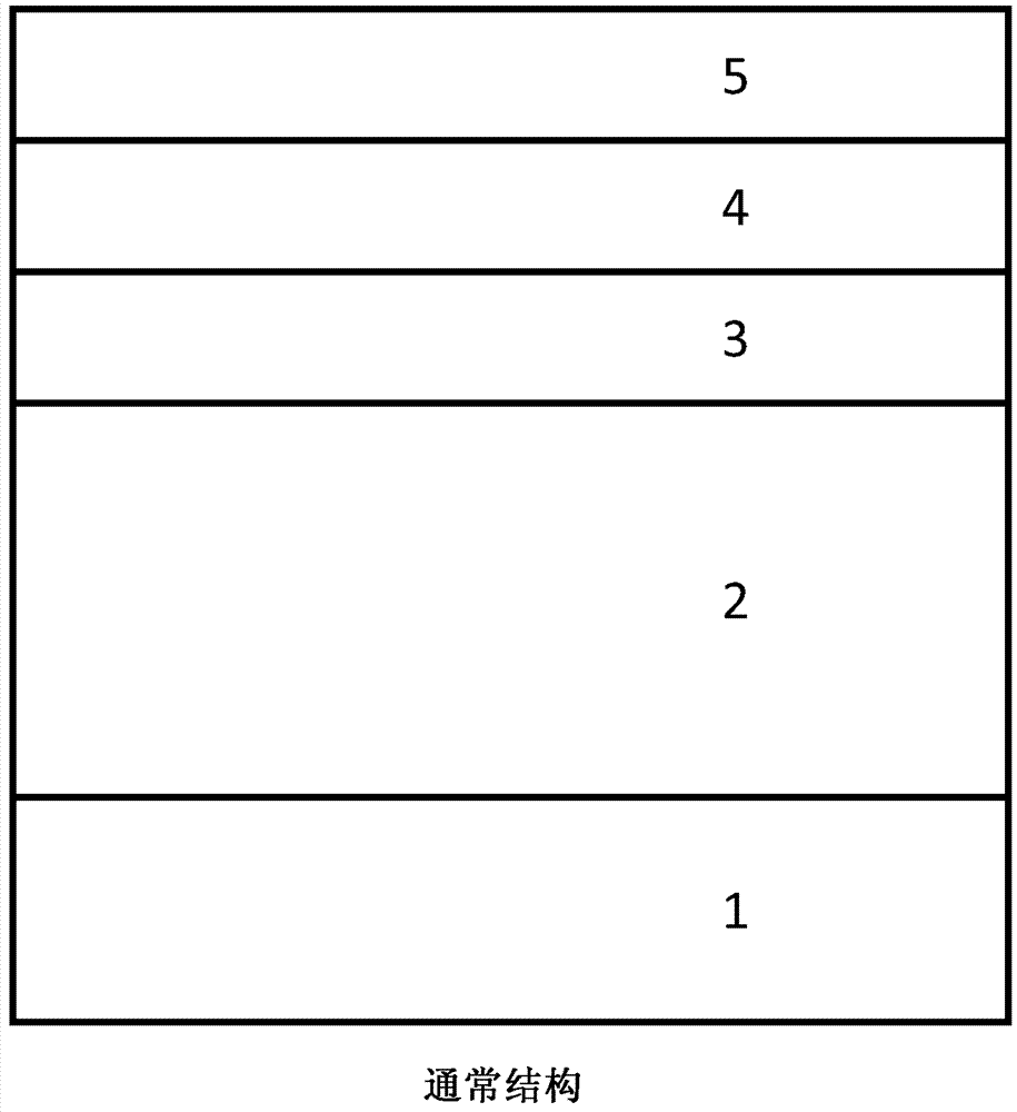
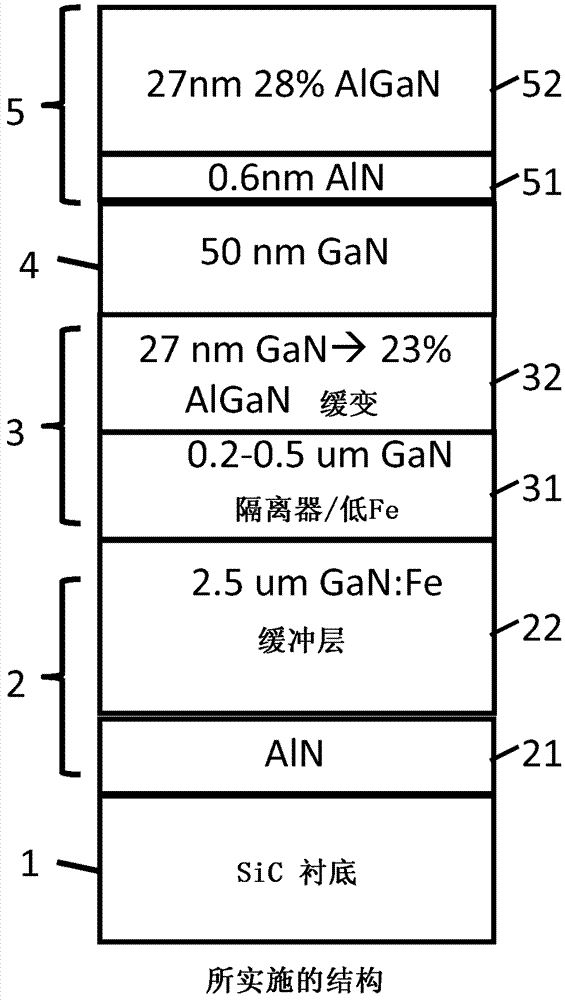
[0022] A device structure in which a dispersed barrier layer is included between the channel layer and the buffer layer of a III-N semiconductor device confines carriers to the channel layer such that dispersion or current collapse due to trapping in the buffer layer is minimized . The term dispersion barrier layer describes a layered structure in a III-N device that reduces electron trapping in the buffer layer and thus reduces drain current dispersion or drain current collapse and increases output. Here, the terms dispersion and current collapse are synonymous for the decrease in drain current due to electron trapping. Additionally, the buffer layer can be made sufficiently insulating, such as by intentional doping to prevent leakage of the buffer layer. To reduce trapping and current collapse, dispersed barrier layers can alleviate the need to grow thick channel or buffer layers. The barrier layer can further eliminate the need to optimize the trade-off between reducing c...


PUM


Abstract

A III-N device is described has a buffer layer, a first III-N material layer on the buffer layer, a second III-N material layer on the first III-N material layer on an opposite side from the buffer layer and a dispersion blocking layer between the buffer layer and the channel layer. The first III-N material layer is a channel layer and a compositional difference between the first III-N material layer and the second III-N material layer induces a 2DEG channel in the first III-N material layer. A sheet or a distribution of negative charge at an interface of the channel layer and the dispersion blocking layer confines electrons away from the buffer layer.

Description

technical field [0001] The present invention relates to a semiconductor device fabricated on a III-nitride semiconductor. Background technique [0002] Ill-nitride-based devices have many potential material advantages over silicon-based devices for high-power electronic applications. Among others, these advantages can include larger bandgap and breakdown field, high electron mobility and low thermally generated current in a two-dimensional electron gas (2DEG). However, for III-nitride semiconductors, large homogeneous substrates are not yet widely used. Currently, Ill-nitride films are still grown by heteroepitaxial growth on suitable non-Ill-nitride substrates. [0003] Substrates commonly used to support III-nitride films are silicon carbide, sapphire, or silicon. Hetero-epitaxy can be performed using molecular beam epitaxy (MBE) or metal oxide chemical vapor deposition (MOCVD), and more recently hydride vapor phase epitaxy (HVPE). It can be difficult to grow high-qual...

Claims


Application Information

Patent Timeline
Patent Type & Authority Patents(China)
IPC IPC(8): H01L29/778H01L21/20
CPCH01L29/7787H01L29/2003H01L29/207H01L29/66462H01L29/205H01L21/02581H01L21/0254
Inventor 乌梅什·米什拉李·麦卡蒂尼古拉斯·菲希坦鲍姆
Owner TRANSPHORM INC
Why Eureka
Try Eureka