Manufacture method of diffractive optical element with large aspect ratio

The technology of a diffractive optical element and a manufacturing method, which is applied in the field of semiconductor microfabrication, can solve the problems of easy collapse of photoresist, and achieve the effect of easy batch preparation

Active Publication Date: 2012-05-23
INST OF MICROELECTRONICS CHINESE ACAD OF SCI
View PDF5 Cites 12 Cited by
  • Summary
  • Abstract
  • Description
  • Claims
  • Application Information

AI Technical Summary

Problems solved by technology

[0006] The main purpose of the present invention is to propose a method for producing a large-aspect-ratio diffractive optical element based on a combination of electron beam lithography and X-ray exposure, so as to solve the problem that the resist is easy to collapse when preparing a large-aspect-ratio diffractive optical element question

Method used


Image

  • Manufacture method of diffractive optical element with large aspect ratio
  • Manufacture method of diffractive optical element with large aspect ratio
  • Manufacture method of diffractive optical element with large aspect ratio

Examples


Embodiment Construction

[0039] In order to make the object, technical solution and advantages of the present invention clearer, the present invention will be described in further detail below in conjunction with specific embodiments and with reference to the accompanying drawings.

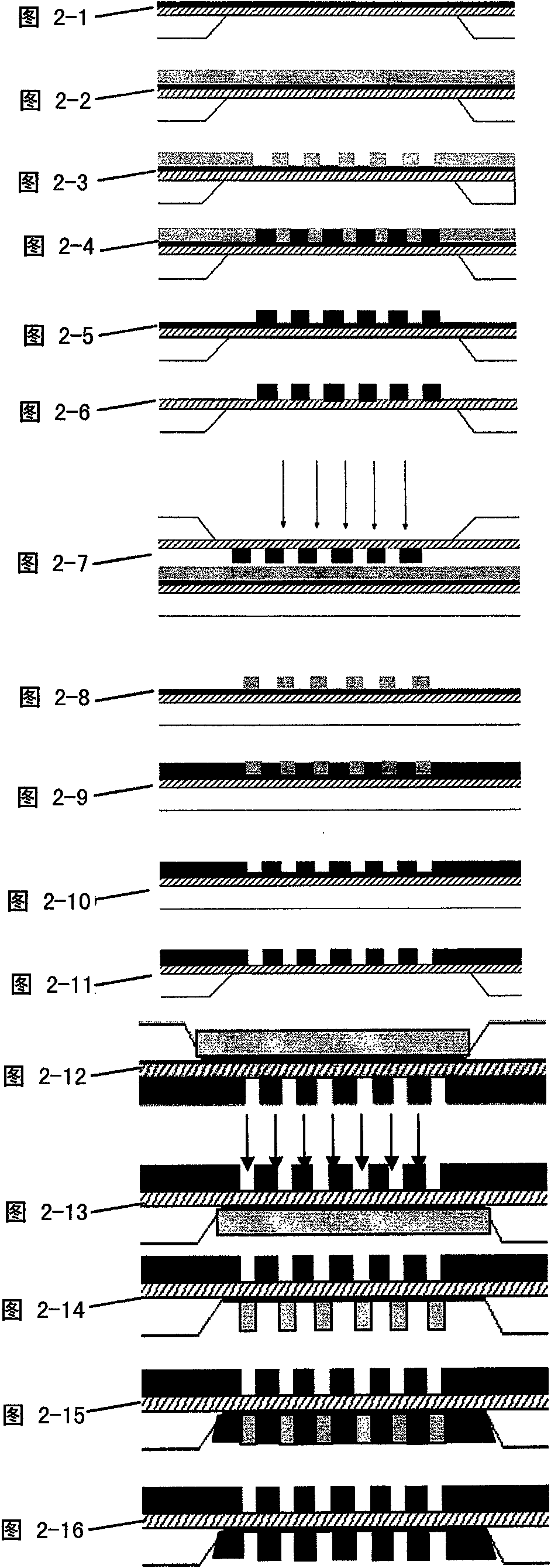
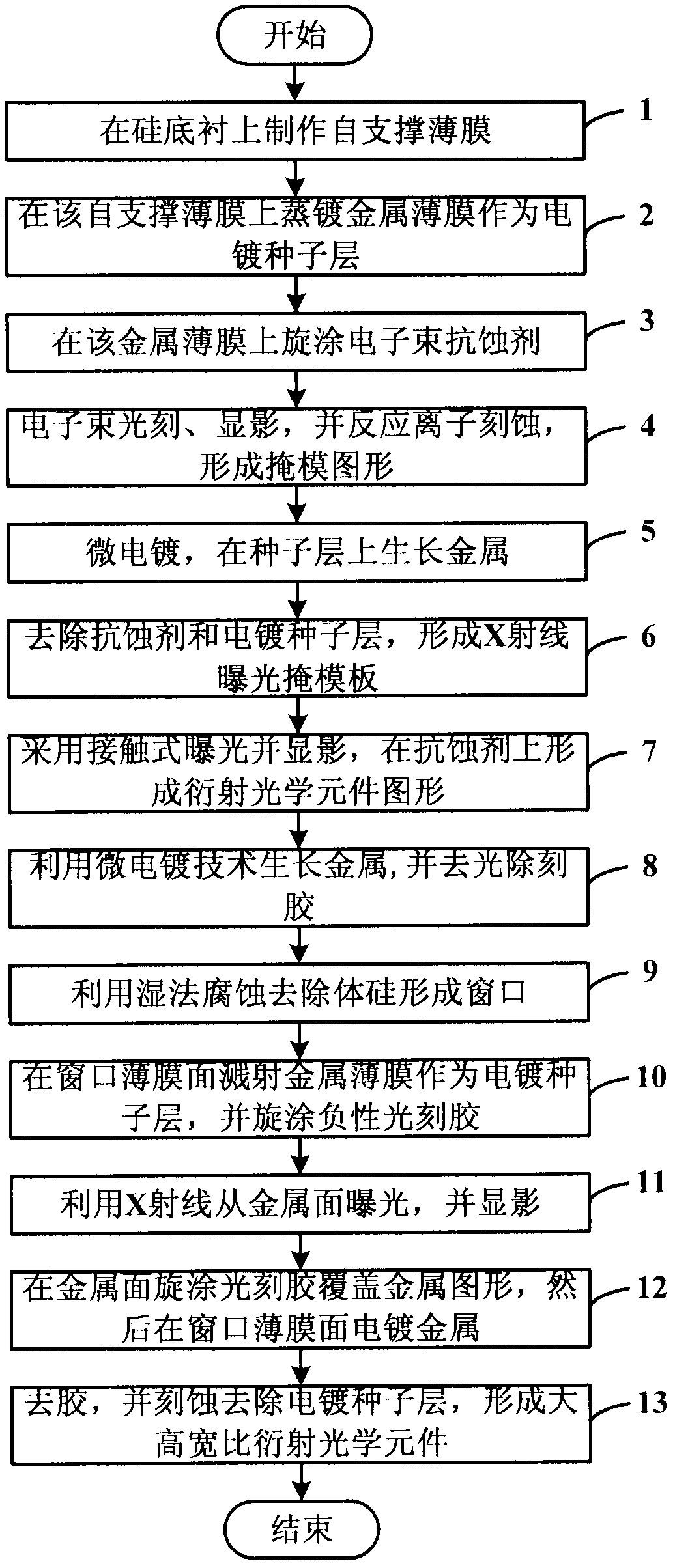
[0040] The method for producing diffractive optical elements with large aspect ratio based on the combination of electron beam lithography and X-ray exposure provided by the present invention uses electron beam direct writing to produce X-ray exposure mask, and uses contact exposure to realize transmission diffractive optics The production of the element involves sputtering and electroplating a seed layer on the surface of the transmissive film substrate, then spin-coating a negative photoresist, exposing it again with X-rays, developing, electroplating, and etching the electroplating seed layer, and then forming a large aspect ratio diffractive optical element.

[0041] Such as figure 1 as shown, figure 1 It is a flow c...


PUM

PropertyMeasurementUnit
thicknessaaaaaaaaaa

Abstract

The invention discloses a manufacture method of a diffractive optical element with large aspect ratio. In the method, an X ray exposure mask is manufactured through electron beam direct writing, a transmission diffractive optical element is manufactured through contact exposure, an electrofacing seed layer is sputtered on a transmission thin film substrate surface, then negative photoresist is coated in a rotating way, X ray is utilized for exposure again, the electroplated and etched electrofacing seed layer is developed, and the diffractive optical element with the large aspect ratio is formed. According to the manufacture method disclosed by the invention, the X ray photoetching mask is prepared through the electron beam direct writing, double exposure utilizing the X ray is carried out, and the diffractive optical element with the large aspect ratio being 10:1 is prepared. The method has the advantages of stability and reliability, easiness in batch preparation, and compatible performance with the traditional photoetching craft.

Description

technical field [0001] The invention relates to the technical field of semiconductor microfabrication, in particular to a method for manufacturing a large aspect ratio diffractive optical element based on the combination of electron beam lithography and X-ray exposure. Background technique [0002] The high aspect ratio diffractive optical element means that the height of the opaque part of the optical element is much larger than its width, usually more than 6:1. Existing methods for making diffractive optical elements with large aspect ratio mainly include multi-layer glue technology and electron beam direct writing thick glue technology. The method has the disadvantages that the graphics are easy to collapse or the development is not complete. [0003] Electron beam lithography, characterized by high resolution, small feature sizes, and pattern-generating capabilities, is a common method for fabricating masks for X-ray lithography. X-rays have extremely high resolution a...

Claims


Application Information

Patent Timeline
Patent Type & Authority Applications(China)
IPC IPC(8): G03F7/00G03F7/20G02B5/18
Inventor 谢常青李海亮史丽娜朱效立刘明
Owner INST OF MICROELECTRONICS CHINESE ACAD OF SCI
Why Eureka
Try Eureka