Method for manufacturing NMOS (N-channel metal oxide semiconductor) transistor

A manufacturing method and transistor technology, applied in semiconductor/solid-state device manufacturing, electrical components, circuits, etc., can solve problems such as insufficient suppression of hot carrier injection effect, improve HCI effect, improve interface quality, and prevent accumulation of charges Effect

Active Publication Date: 2014-09-03
SEMICONDUCTOR MANUFACTURING INTERNATIONAL (BEIJING) CORP
View PDF4 Cites 0 Cited by
  • Summary
  • Abstract
  • Description
  • Claims
  • Application Information

AI Technical Summary

Problems solved by technology

However, in the above technologies, as the size of semiconductor devices continues to shrink, for example, in semiconductor devices with a size of 65nm and below, the above technical solutions are not enough to suppress the hot carrier injection effect, so they are not applicable

Method used


Image

  • Method for manufacturing NMOS (N-channel metal oxide semiconductor) transistor
  • Method for manufacturing NMOS (N-channel metal oxide semiconductor) transistor
  • Method for manufacturing NMOS (N-channel metal oxide semiconductor) transistor

Examples


Embodiment Construction

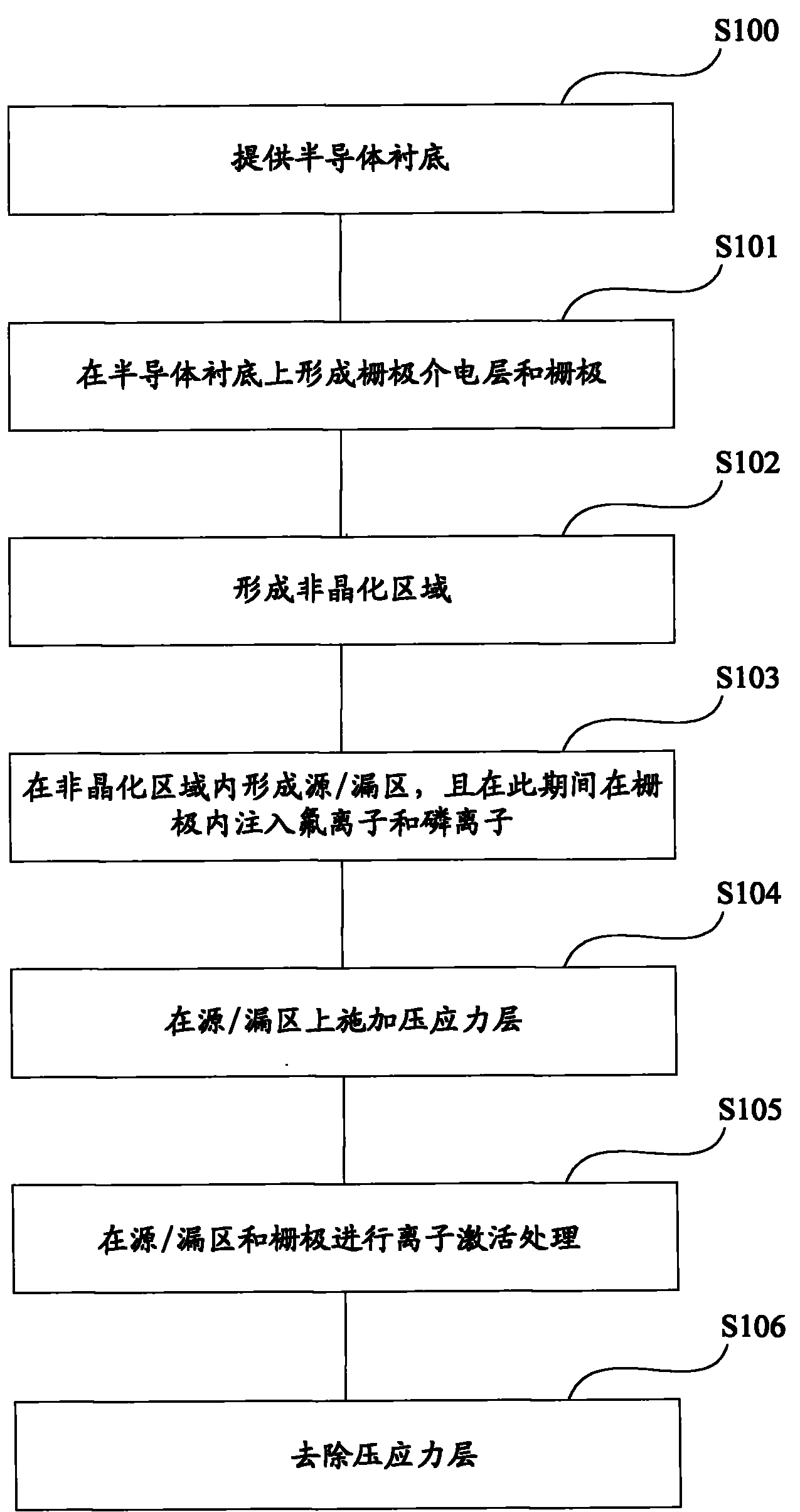
[0026] In order to make the above objects, features and advantages of the present invention more comprehensible, specific implementations of the present invention will be described in detail below in conjunction with the accompanying drawings.

[0027] In the following description, many specific details are set forth in order to fully understand the present invention, but the present invention can also be implemented in other ways than those described here, so the present invention is not limited by the specific embodiments disclosed below.

[0028] As mentioned in the background technology section, HCI is due to the presence of a strong lateral electric field in the NMOS transistor, which causes the impact ionization of the carriers during the transport process, generating additional electron-hole pairs, and part of the hot carriers are injected into the gate. In the oxide layer or gate, resulting in HCI effect.

[0029] Therefore, when manufacturing a semiconductor device, i...


PUM


Abstract

The invention discloses a method for manufacturing an NMOS (N-channel metal oxide semiconductor) transistor, which belongs to the technical field of semiconductors. The method comprises the following steps of: providing a semiconductor substrate; forming a grid dielectric layer and a grid positioned on the grid dielectric layer on the semiconductor substrate; carrying out non-crystallizing on the semiconductor substrate by taking the grid dielectric layer and the grid as masks to form a non-crystallized region; forming a source / drain region in the non-crystallized region, and implanting fluorine ions and phosphorous ions into the grid in the process of forming the source / drain region; applying a pressure stress layer to the source / drain region; activating ions of the source / drain region and the grid; and removing the pressure stress layer. The fluorine ions are implanted into the grid, enter the grid dielectric layer and replace part of oxygen ions in the grid dielectric layer to form a fluorine silicon group, so that the quality of the interface between the grid dielectric layer and the semiconductor substrate is improved, and the hot carrier implanting effect of the NMOS transistor is improved.

Description

technical field [0001] The invention relates to a manufacturing method in the technical field of semiconductors, in particular to a manufacturing method of an NMOS transistor. Background technique [0002] With the continuous improvement of the integration level of semiconductor devices, the feature size is gradually reduced, and the source / drain and the source / drain extension (Source / Drain Extension) become shallower accordingly. The current technology level requires the source / drain of semiconductor devices Junction depths are less than 1000 Angstroms, and junction depths on the order of 200 Angstroms or less may ultimately be required. [0003] The reduction of the junction depth requires a lower heat treatment temperature, and the lower heat treatment temperature (less than 500 degrees Celsius, or even lower) reduces the lateral size of the junction, and the reduction of the lateral size of the junction will lead to a device in the The electric field formed between the ...

Claims


Application Information

Patent Timeline
Patent Type & Authority Patents(China)
IPC IPC(8): H01L21/336H01L21/265
Inventor 谢欣云卢炯平陈志豪
Owner SEMICONDUCTOR MANUFACTURING INTERNATIONAL (BEIJING) CORP
Why Eureka
Try Eureka