Manufacturing method for semiconductor device

A manufacturing method and semiconductor technology, applied in the direction of semiconductor/solid-state device manufacturing, electrical components, circuits, etc., to achieve the effect of improving HCI effect, low cost, and improving interface quality

Active Publication Date: 2014-03-12
SEMICON MFG INT (BEIJING) CORP
View PDF5 Cites 0 Cited by
  • Summary
  • Abstract
  • Description
  • Claims
  • Application Information

AI Technical Summary

Problems solved by technology

But this method only works for PMOS transistors

Method used


Image

  • Manufacturing method for semiconductor device
  • Manufacturing method for semiconductor device
  • Manufacturing method for semiconductor device

Examples


Embodiment 1

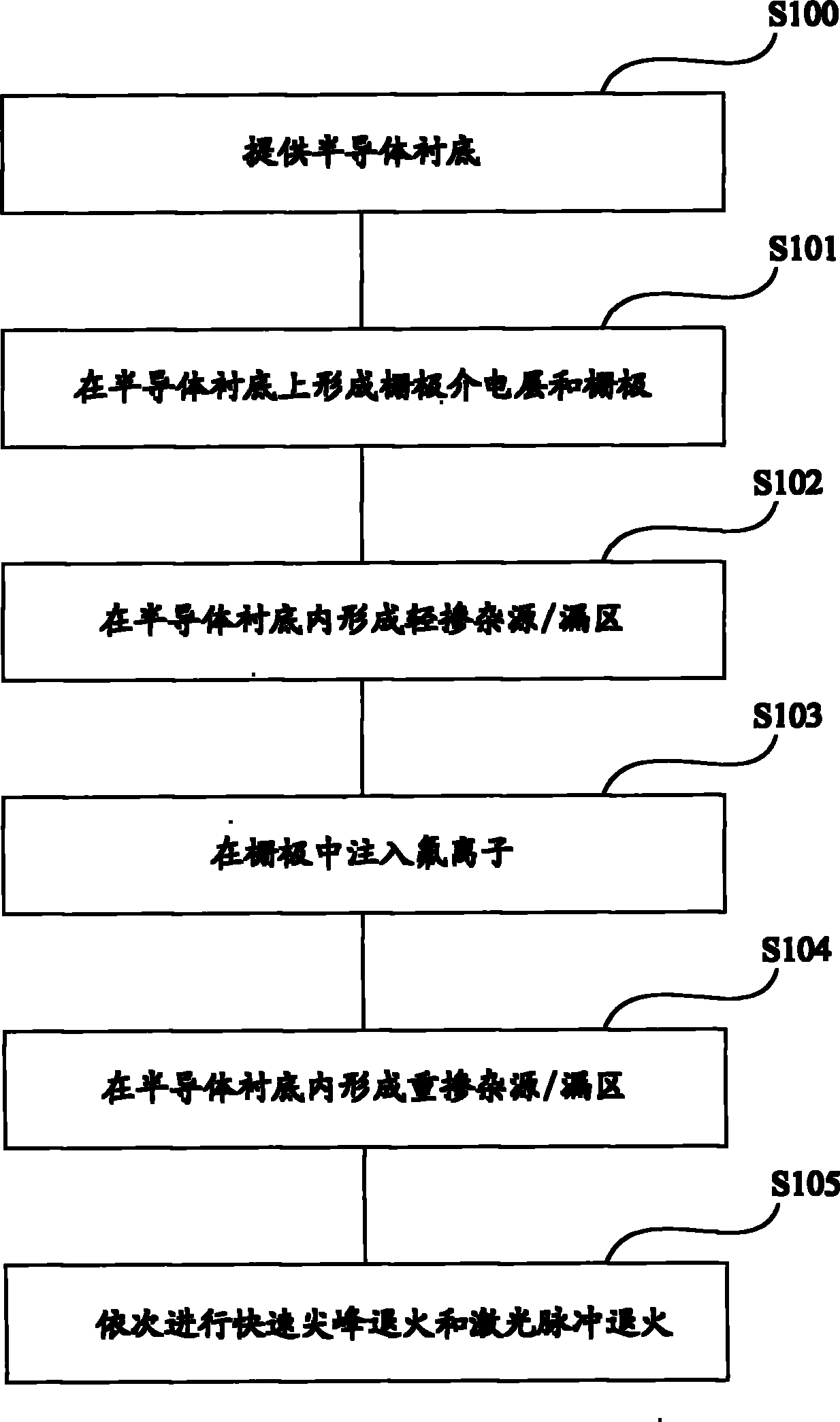
[0032] Such as figure 1 As shown, the manufacturing method of the semiconductor device in this embodiment includes the following steps:

[0033] S100, providing a semiconductor substrate;

[0034] S101, forming a gate dielectric layer and a gate on the gate dielectric layer on the semiconductor substrate;

[0035] S102, performing lightly doped ion implantation in the semiconductor substrate on both sides of the gate to form lightly doped source / drain regions;

[0036] S103, implanting fluorine ions into the gate;

[0037] S104, performing heavily doped ion implantation in the semiconductor substrate on both sides of the gate to form heavily doped source / drain regions;

[0038] S105, performing rapid spike annealing and laser pulse annealing in sequence.

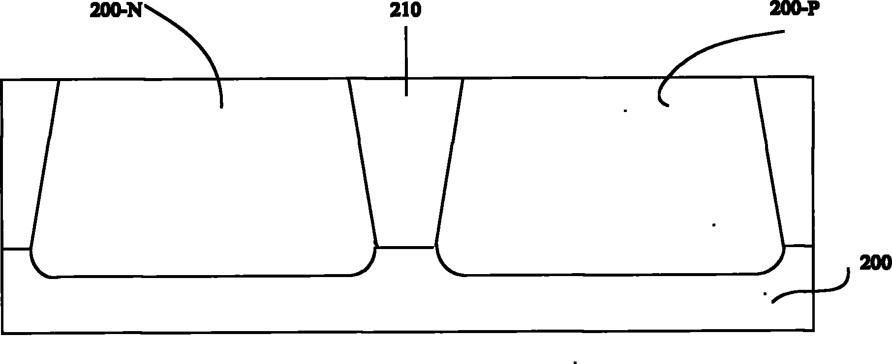
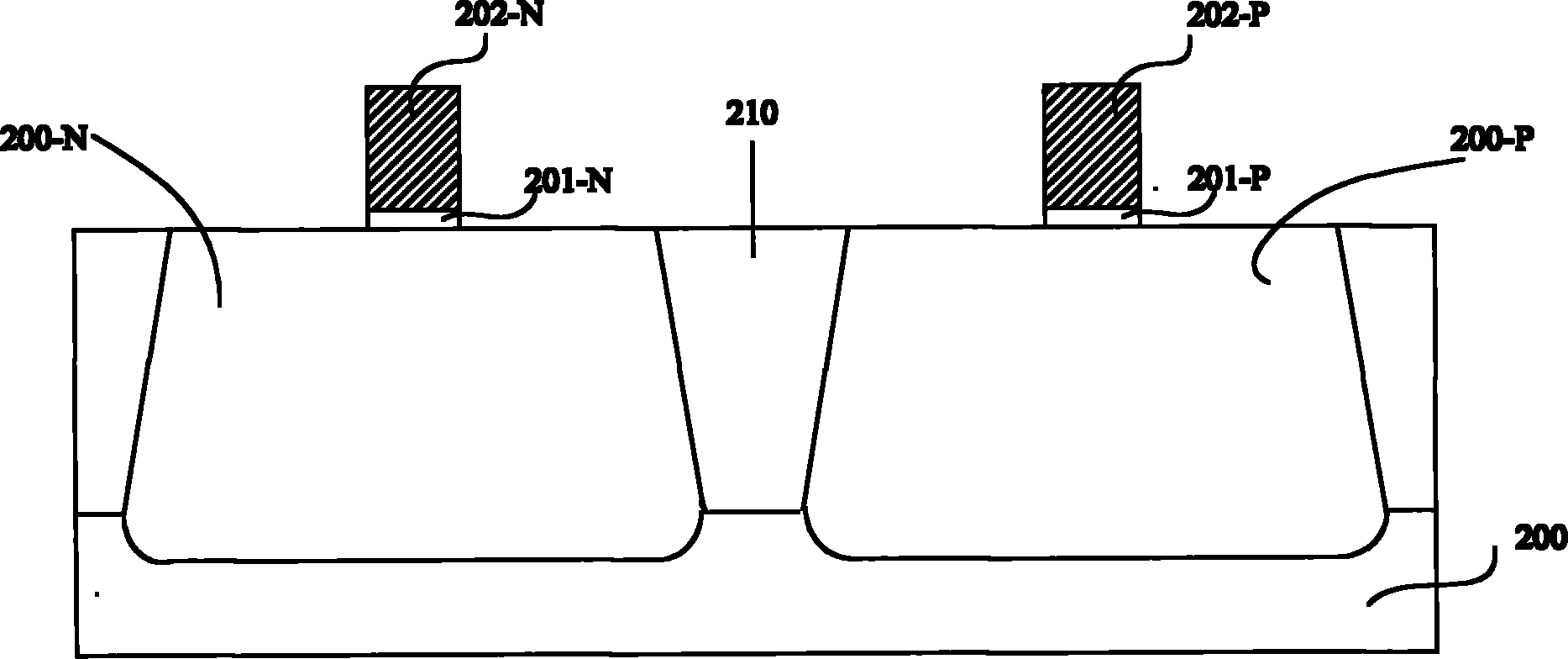
[0039] refer to figure 2 , first execute step S100 to provide a semiconductor substrate 200 . Wherein, the semiconductor substrate 200 includes: an N-type doped well 200 -N, a P-type doped well 200 -P and an isolation...

Embodiment 2

[0060] Such as Figure 10 As shown, the manufacturing method of the semiconductor device in this embodiment includes the following steps:

[0061]S300, providing a semiconductor substrate;

[0062] S301, forming a gate dielectric layer and a gate on the gate dielectric layer on the semiconductor substrate;

[0063] S302, performing lightly doped ion implantation in the semiconductor substrate on both sides of the gate to form lightly doped source / drain regions;

[0064] S303, performing heavily doped ion implantation in the semiconductor substrate on both sides of the gate to form heavily doped source / drain regions;

[0065] S304, implanting fluorine ions into the gate;

[0066] S305, performing rapid spike annealing and laser pulse annealing in sequence.

[0067] The difference between this embodiment and Embodiment 1 lies in the steps of "implanting heavily doped ions into the semiconductor substrate on both sides of the gate to form heavily doped source / drain regions" a...

Embodiment 3

[0070] Such as Figure 11 As shown, the manufacturing method of the semiconductor device in this embodiment includes the following steps:

[0071] S400, providing a semiconductor substrate;

[0072] S401, forming a gate dielectric layer and a gate on the gate dielectric layer on the semiconductor substrate;

[0073] S402, implanting fluorine ions into the gate;

[0074] S403, performing lightly doped ion implantation in the semiconductor substrate on both sides of the gate to form lightly doped source / drain regions;

[0075] S404, performing heavily doped ion implantation in the semiconductor substrate on both sides of the gate to form heavily doped source / drain regions;

[0076] S405, performing rapid spike annealing and laser pulse annealing in sequence.

[0077] The difference between this embodiment and Embodiment 1 is only in the steps of "implanting lightly doped ions into the semiconductor substrate on both sides of the gate to form lightly doped source / drain region...


PUM


Abstract

The invention discloses a manufacturing method for a semiconductor device, and belongs to the technical field of semiconductors. The method comprises the following steps of: providing a semiconductor substrate; forming a gate dielectric layer and a gate positioned on the gate dielectric layer on the semiconductor substrate; forming source / drain areas in the semiconductor substrate of two sides of the gate, and injecting fluorine ions during forming of the source / drain areas; and sequentially performing fast peak annealing and laser pulse annealing after the source / drain areas are formed. The fluorine ions enter the gate dielectric layer, and replace a part of oxygen ions in the gate dielectric layer to form fluorine and silicon groups, so the hot carrier injection (HCI) effect of an N-channel metal oxide semiconductor (NMOS) transistor and a negative bias temperature instability (NBTI) effect of a P-channel metal oxide semiconductor (PMOS) are improved.

Description

technical field [0001] The invention relates to a manufacturing method in the field of semiconductor technology, in particular to a manufacturing method of a semiconductor device including an NMOS transistor and a PMOS transistor. Background technique [0002] With the development of technology, the size of semiconductor devices continues to decrease, the HCI (Hot Carrier Injection, hot carrier injection) effect of NMOS transistors and the NBTI (Negative Bias Temperature Instability, negative bias instability) effect of PMOS transistors follow. It is becoming more and more serious and has become a major problem affecting the reliability of semiconductor devices. [0003] With the shrinking of the channel length of semiconductor devices, in order to obtain the required driving current and suppress the short channel effect, the semiconductor substrate and the source and drain are usually doped with a higher concentration, resulting in the depletion region of the source and dra...

Claims


Application Information

Patent Timeline
Patent Type & Authority Patents(China)
IPC IPC(8): H01L21/8238H01L21/265H01L21/324
Inventor 谢欣云陈志豪卢炯平
Owner SEMICON MFG INT (BEIJING) CORP
Why Eureka
Try Eureka