Manufacturing method of NMOS (N-channel metal oxide semiconductor) transistor

A manufacturing method and transistor technology, applied in semiconductor/solid-state device manufacturing, electrical components, circuits, etc., can solve problems such as insufficient suppression of hot carrier injection effects, improve HCI effects, improve interface quality, and prevent accumulation of charges Effect

Active Publication Date: 2013-09-04
SEMICONDUCTOR MANUFACTURING INTERNATIONAL (BEIJING) CORP
View PDF1 Cites 0 Cited by
  • Summary
  • Abstract
  • Description
  • Claims
  • Application Information

AI Technical Summary

Problems solved by technology

However, in the above technologies, as the size of semiconductor devices continues to shrink, for example, in semiconductor devices with a size of 65nm and below, the above technical solutions are not enough to suppress the hot carrier injection effect, so they are not applicable

Method used


Image

  • Manufacturing method of NMOS (N-channel metal oxide semiconductor) transistor
  • Manufacturing method of NMOS (N-channel metal oxide semiconductor) transistor
  • Manufacturing method of NMOS (N-channel metal oxide semiconductor) transistor

Examples


Embodiment 1

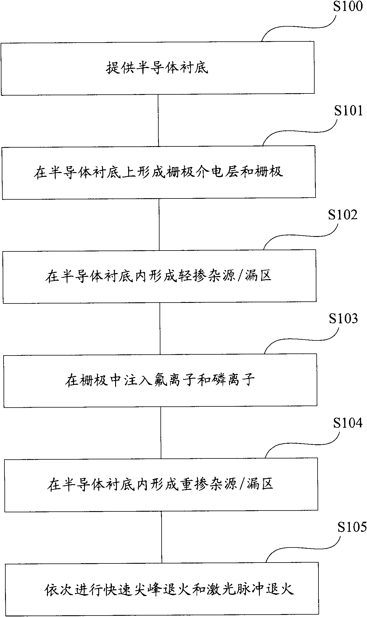
[0028] Such as figure 1 As shown, the manufacturing method of the NMOS transistor in this embodiment includes the following steps:

[0029] S100, providing a semiconductor substrate;

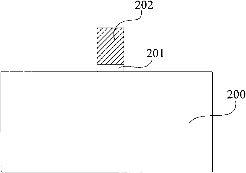
[0030] S101, forming a gate dielectric layer and a gate on the gate dielectric layer on the semiconductor substrate;

[0031] S102, performing lightly doped ion implantation in the semiconductor substrate on both sides of the gate to form lightly doped source / drain regions;

[0032] S103, implanting fluorine ions and phosphorus ions into the gate;

[0033] S104, performing heavily doped ion implantation in the semiconductor substrate on both sides of the gate to form heavily doped source / drain regions;

[0034] S105, performing rapid spike annealing and laser pulse annealing in sequence.

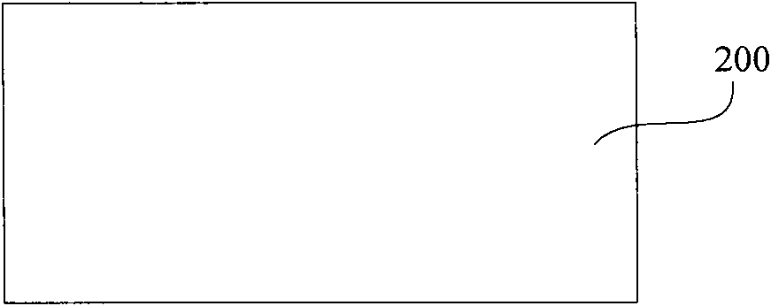
[0035] refer to figure 2 , first execute step S100 to provide a semiconductor substrate 200 . Wherein, the semiconductor substrate 200 is silicon formed with semiconductor devices, silicon-on-insulator ...

Embodiment 2

[0057] Such as Figure 10 As shown, the manufacturing method of the NMOS transistor in this embodiment includes the following steps:

[0058] S300, providing a semiconductor substrate;

[0059] S301, forming a gate dielectric layer and a gate on the gate dielectric layer on the semiconductor substrate;

[0060] S302, performing lightly doped ion implantation in the semiconductor substrate on both sides of the gate to form lightly doped source / drain regions;

[0061] S303, performing heavily doped ion implantation in the semiconductor substrate on both sides of the gate to form heavily doped source / drain regions;

[0062] S304, implanting fluorine ions and phosphorus ions into the grid;

[0063] S305, performing rapid spike annealing and laser pulse annealing in sequence.

[0064] The difference between this embodiment and Embodiment 1 lies in the steps of "implanting heavily doped ions into the semiconductor substrate on both sides of the gate to form heavily doped source / ...

Embodiment 3

[0067] Such as Figure 11 As shown, the manufacturing method of the NMOS transistor in this embodiment includes the following steps:

[0068] S400, providing a semiconductor substrate;

[0069] S401, forming a gate dielectric layer and a gate on the gate dielectric layer on the semiconductor substrate;

[0070] S402, implanting fluorine ions and phosphorus ions into the grid;

[0071] S403, performing lightly doped ion implantation in the semiconductor substrate on both sides of the gate to form lightly doped source / drain regions;

[0072] S404, performing heavily doped ion implantation in the semiconductor substrate on both sides of the gate to form heavily doped source / drain regions;

[0073] S405, performing rapid spike annealing and laser pulse annealing in sequence.

[0074] The difference between this embodiment and Embodiment 1 is only in the steps of "implanting lightly doped ions into the semiconductor substrate on both sides of the gate to form lightly doped sour...


PUM


Abstract

The invention discloses a manufacturing method of a NMOS (N-channel metal oxide semiconductor) transistor in the technical field of semiconductors. The manufacturing method comprises the following steps of: providing a semiconductor substrate; forming a gate dielectric layer on the semiconductor substrate and forming a gate positioned on the gate dielectric layer; forming source / drain regions in the semiconductor substrate on the two sides of the gate, implanting fluorine ions and phosphorus ions into the gate during the period of forming the source / drain regions; and after forming the source / drain regions, performing rapid spike annealing and laser pulse annealing in sequence. In the manufacturing method, the fluorine ions enter the gate dielectric layer, and the fluorine ions replace a part of oxygen ions in the gate dielectric layer to form fluorine-silicon groups, which improves quality of the interface between the gate dielectric layer and the semiconductor substrate, so as to improve the hot carrier injection effect.

Description

technical field [0001] The invention relates to a device manufacturing method in the field of semiconductor technology, in particular to a manufacturing method of an NMOS transistor. Background technique [0002] With the continuous improvement of the integration level of semiconductor devices, the feature size is gradually reduced, and the source / drain and the source / drain extension (Source / Drain Extension) become shallower accordingly. The current technology level requires the source / drain of semiconductor devices Junction depths are less than 1000 Angstroms, and junction depths on the order of 200 Angstroms or less may ultimately be required. [0003] The reduction of the junction depth requires a lower heat treatment temperature, and the lower heat treatment temperature (less than 500 degrees Celsius, or even lower) reduces the lateral size of the junction, and the reduction of the lateral size of the junction will lead to a device in the The electric field formed betwe...

Claims


Application Information

Patent Timeline
Patent Type & Authority Patents(China)
IPC IPC(8): H01L21/336H01L21/265
Inventor 谢欣云陈志豪卢炯平
Owner SEMICONDUCTOR MANUFACTURING INTERNATIONAL (BEIJING) CORP
Why Eureka
Try Eureka