Method for forming dual damascene structure and semiconductor device

A dual damascene structure, semiconductor technology, applied in the direction of semiconductor devices, semiconductor/solid-state device manufacturing, semiconductor/solid-state device parts, etc. Problems such as poor layer adhesion

Active Publication Date: 2012-05-23
SEMICONDUCTOR MANUFACTURING INTERNATIONAL (BEIJING) CORP
View PDF5 Cites 4 Cited by
  • Summary
  • Abstract
  • Description
  • Claims
  • Application Information

AI Technical Summary

Problems solved by technology

[0009] The problem solved by the present invention is that the adhesion between the second dielectric layer and the diffusion barrier layer is poor, and it is easy to cause delamination of the second dielectric layer and the diffusion barrier layer

Method used


Image

  • Method for forming dual damascene structure and semiconductor device
  • Method for forming dual damascene structure and semiconductor device
  • Method for forming dual damascene structure and semiconductor device

Examples


Embodiment Construction

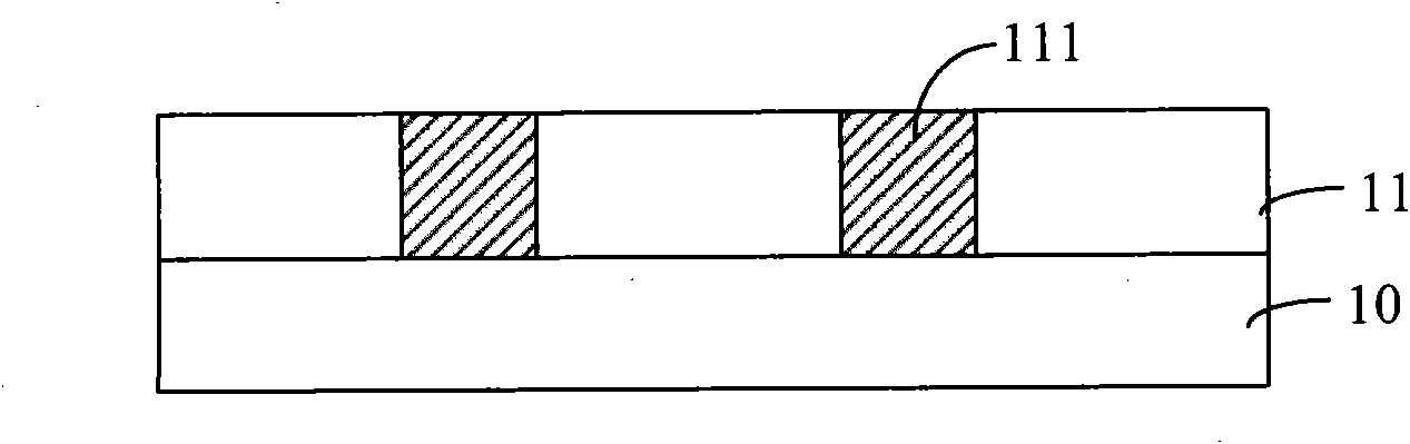
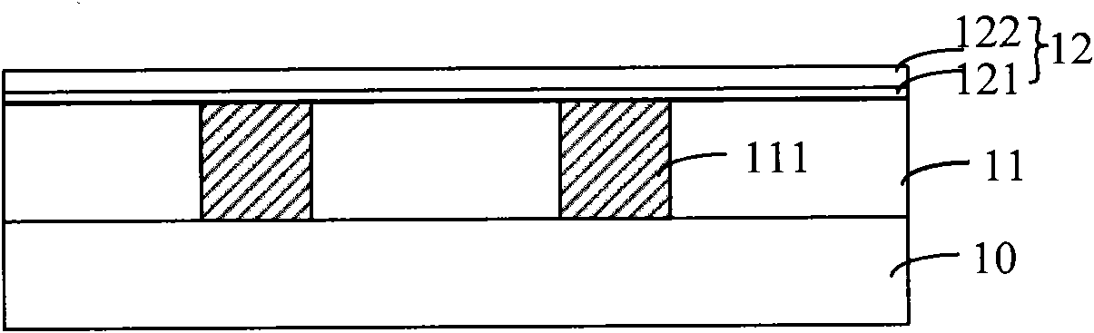
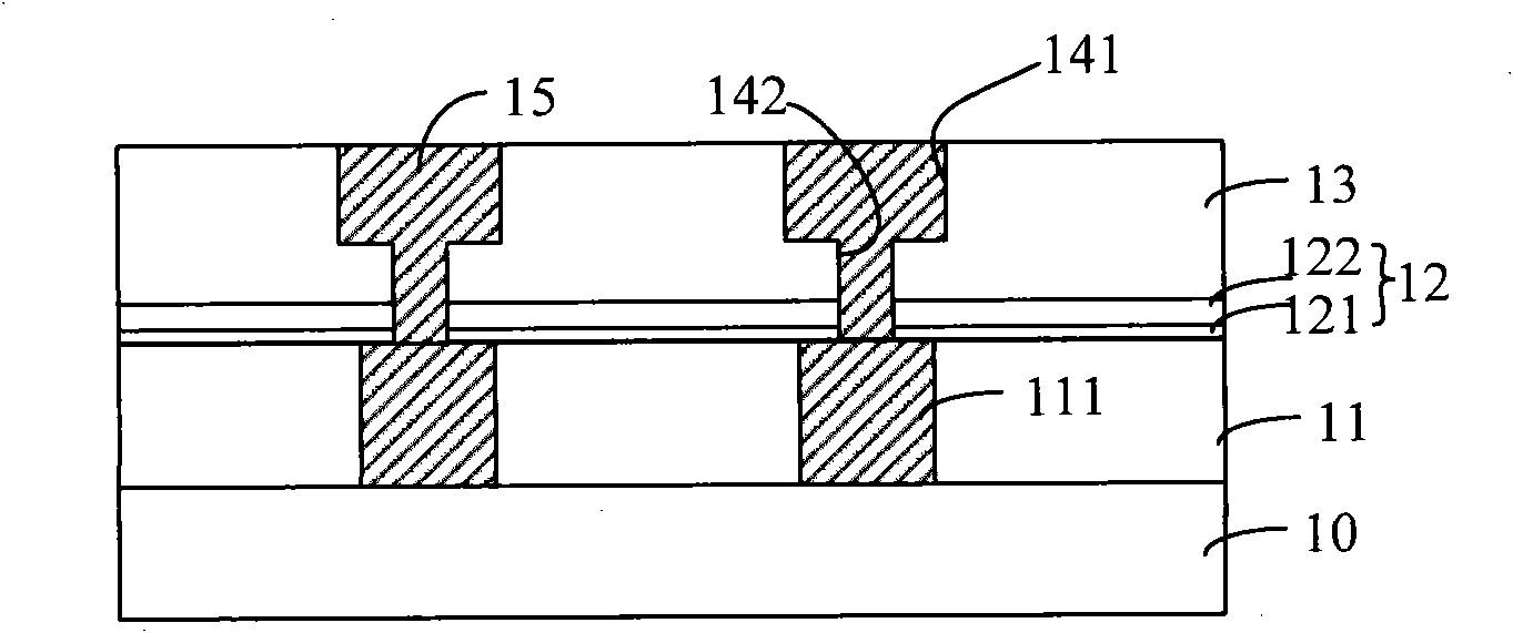
[0044] After a long period of research, the inventor found that due to the large stress difference between the second nitrogen-doped silicon carbide layer and the low-k second dielectric layer, the gap between the second nitrogen-doped silicon carbide layer and the low-k second dielectric layer Poor adhesion, prone to delamination problems.

[0045] According to the method for forming a dual damascene structure and the method for forming a semiconductor device according to the specific embodiment of the present invention, a stress buffer layer is formed between the nitrogen-doped silicon carbide layer and the low-k second dielectric layer, and the stress buffer layer and the nitrogen-doped The stress difference between the silicon carbide layer and the low-k second dielectric layer is small, and the adhesion between them is good.

[0046] In order to enable those skilled in the art to better understand the present invention, specific embodiments of the present invention will b...


PUM

PropertyMeasurementUnit
thicknessaaaaaaaaaa
thicknessaaaaaaaaaa

Abstract

A method for forming a dual damascene structure and a semiconductor device are disclosed. The method comprises the following steps: providing a substrate, wherein a first dielectric layer and a nitrating silicon carbide layer are successively formed on the substrate; forming a stress buffer layer on the nitrating silicon carbide layer; forming a second dielectric layer on the stress buffer layer, wherein a dielectric constant of the second dielectric layer is less than 3.5; etching the second dielectric layer, the stress buffer layer and the nitrating silicon carbide layer so as to form an interconnection groove and an interconnection through hole; filling metal in the interconnection groove and an interconnection through hole so as to form the dual damascene structure. By using the method and the device of the invention, the second dielectric layer and the nitrating silicon carbide layer can not generate spalling.

Description

technical field [0001] The invention relates to the technical field of semiconductors, in particular to a method for forming a double damascene structure and a semiconductor device. Background technique [0002] With the development of semiconductor technology, the integration level of integrated circuits is getting higher and higher, and the feature size (CD) of devices is getting smaller and smaller. Towards low-k (dielectric constant) materials. [0003] In the prior art, the method for forming a dual damascene structure in a low-k dielectric layer is: [0004] refer to Figure 1a , providing a substrate 10, a first dielectric layer 11 is formed on the substrate 10, the material of the first dielectric layer 11 is SiOCH (silicon oxycarbide), and a copper interconnection structure 111 is formed in the first dielectric layer 11, the The copper interconnection structure is a dual damascene structure, and may also be other interconnection structures. The figure is only sche...

Claims


Application Information

Patent Timeline
Patent Type & Authority Applications(China)
IPC IPC(8): H01L21/768H01L23/522H01L23/532
Inventor 周鸣
Owner SEMICONDUCTOR MANUFACTURING INTERNATIONAL (BEIJING) CORP
Why Eureka
Try Eureka