Super junction semiconductor element and manufacture method thereof

A manufacturing method and semiconductor technology, applied in semiconductor/solid-state device manufacturing, semiconductor devices, electrical components, etc., can solve the problems of affecting device reliability, high cost, and high process difficulty, avoiding excessive epitaxy times and reducing warpage. , the effect of reducing the difficulty of the process

Inactive Publication Date: 2012-05-30
BYD CO LTD
View PDF5 Cites 27 Cited by
  • Summary
  • Abstract
  • Description
  • Claims
  • Application Information

AI Technical Summary

Problems solved by technology

[0010] The technical problem solved by the present invention is that the pure multiple epitaxy method in the prior art causes lattice defects and affects the

Method used


Image

  • Super junction semiconductor element and manufacture method thereof
  • Super junction semiconductor element and manufacture method thereof
  • Super junction semiconductor element and manufacture method thereof

Examples


Embodiment 1

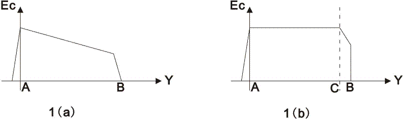
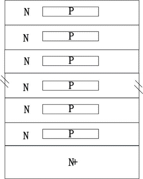
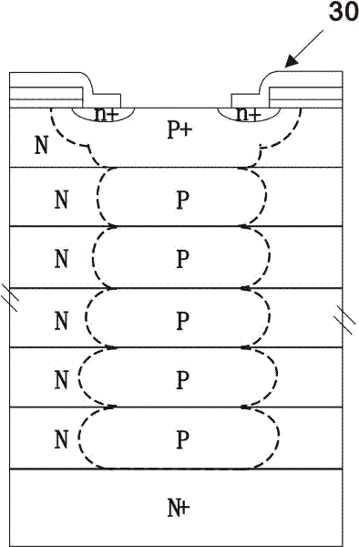
[0026] refer to Figure 12 , a super junction semiconductor element, comprising: a first conductivity type substrate 11; at least one layer of a first conductivity type first epitaxial layer 12 disposed on the first conductivity type substrate, the first epitaxial layer comprising The second conductivity type doping 122; the first conductivity type second epitaxial layer 13 disposed on the first conductivity type first epitaxial layer; the second epitaxial layer includes the second conductivity type doping 132; the second epitaxial layer A device feature layer 100 is disposed on it.

[0027] A method for manufacturing the above-mentioned super junction semiconductor element, its flow chart is as follows Figure 7 to Figure 12 As shown, it includes: step 1: providing a substrate of the first conductivity type; step 2: growing a first epitaxial layer of the first conductivity type on the substrate of the first conductivity type, and performing doping of the second conductivity ty...

Embodiment 2

[0044] refer to Figure 18 , a super junction semiconductor element, comprising: a substrate of a first conductivity type; a third epitaxial layer of the first conductivity type disposed on the substrate of the first conductivity type, wherein the third epitaxial layer includes doped materials of the second conductivity type heterogeneous; at least one fourth epitaxial layer of the first conductivity type disposed on the first epitaxial layer of the first conductivity type; the fourth epitaxial layer includes doping of the second conductivity type; device features are arranged on the fourth epitaxial layer Floor.

[0045] A method for manufacturing the above-mentioned super junction semiconductor element, comprising: step 1: providing a substrate of the first conductivity type; step 2: growing a third epitaxial layer of the first conductivity type on the substrate of the first conductivity type; layer, and make the second conductivity type doping in the etched groove; Step 3:...


PUM

PropertyMeasurementUnit
Thicknessaaaaaaaaaa
Thicknessaaaaaaaaaa

Abstract

The invention relates to a super junction semiconductor element and a manufacture method thereof. The super junction semiconductor element comprises a first conduction type substrate, at least one first conduction type first epitaxial layer and at least one first conduction type second epitaxial layer, wherein the first conduction type first epitaxial layer is arranged on the first conduction type substrate and comprises second conduction type doping, the first conduction type second epitaxial layer is arranged on the first conduction type first epitaxial layer and comprises second conduction type doping, and a device characteristic layer is arranged on the second epitaxial layer. The lattice defect problem caused by multi-time epitaxial growth, ion injection and diffusion can also be reduced to a certain degree, and high cost generated by too many epitaxial times is avoided. Simultaneously, the process difficulty of the etching and the groove filling is also greatly reduced along with grooves, and the stress and wafer curling problems caused by excessive depth of the grooves are also reduced.

Description

technical field [0001] The invention belongs to the field of semiconductor manufacturing, and in particular relates to a super junction semiconductor element and a manufacturing method thereof. Background technique [0002] In common power devices, the reverse voltage that determines the N+ region and the P+ region is borne by a lightly doped semiconductor, and this layer is called the Voltage Sustaining Layer (Voltage Sustaining Layer) below. For high-voltage power devices, the on-resistance Ron (or on-voltage drop) is also mainly determined by the withstand voltage layer. The lighter the doping of this layer, or the greater the thickness, or both, the higher the breakdown voltage. But the on-resistance (or on-voltage drop) is also larger. One of the most important issues in power devices is to have both high breakdown voltage and low on-resistance, and the relationship between the two becomes an obstacle to fabricate high-performance power devices. Modern common power se...

Claims


Application Information

Patent Timeline
IPC IPC(8): H01L29/12H01L21/336H01L21/20H01L21/306
Inventor 朱超群任文珍钟树理陈宇曾爱平
Owner BYD CO LTD
Why Eureka
Try Eureka