Zener diode protection network in submount for leds connected in series
A zener diode and light emitting diode technology, which is applied in the use of semiconductor lamps, electrical components, circuits, etc., can solve the problems of insufficient surface area of zener diode silicon
- Summary
- Abstract
- Description
- Claims
- Application Information
AI Technical Summary
Problems solved by technology
Method used
Image

Examples
Embodiment Construction
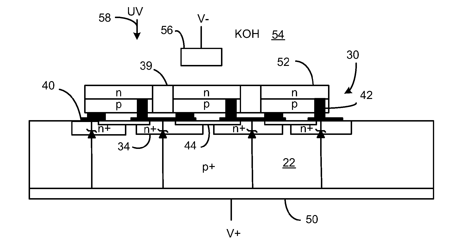
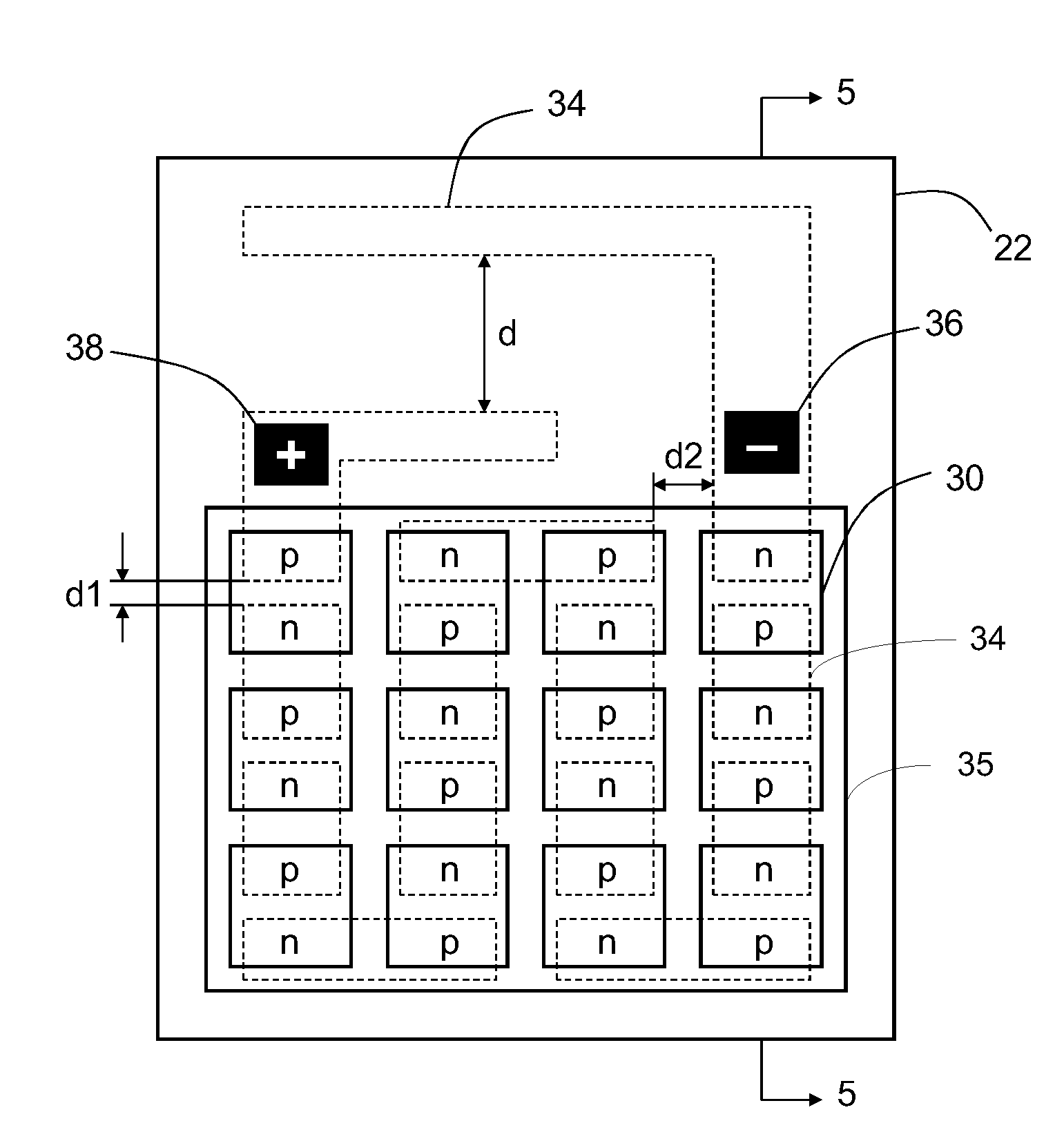
[0027] As a preliminary matter, LEDs were formed on a growth substrate. In the example used, the LEDs are GaN-based LEDs, such as AlInGaN or InGaN LEDs, which are used to generate UV by green light. Typically, a relatively thick n-type GaN layer is grown on a sapphire growth substrate using conventional techniques. Relatively thick GaN layers typically include a low temperature nucleation layer and one or more additional layers to provide a low defect lattice structure for the n-type cladding layer and active layer. Then, one or more n-type cladding layers are formed over the thick n-type layer, followed by the active layer, one or more p-type cladding layers, and a p-type contact layer (for metallization).
[0028] For flip-chip, portions of the p-layer and active layer are etched away to expose the n-layer for metallization. In this way, the p-contact and n-contact are on the same side of the chip and can be electrically attached directly to the substrate contact pads. Cu...
PUM
 Abstract
Description
Claims
Application Information