High-voltage transient voltage suppressor chip and production process

A technology of transient voltage suppression and production technology, which is applied in semiconductor/solid-state device manufacturing, circuits, electrical components, etc. It can solve problems such as poor anti-surge capability, affect product reliability, chip damage, etc., and improve withstand voltage performance , Improving the effect of anti-surge capability and reliability

Active Publication Date: 2012-07-04
TIANJIN ZHONGHUAN SEMICON CO LTD
View PDF3 Cites 29 Cited by
  • Summary
  • Abstract
  • Description
  • Claims
  • Application Information

AI Technical Summary

Problems solved by technology

There are problems in the existing technology: when a single diffusion junction is used in the production of transient voltage suppressor chips, if the reverse breakdown voltage reaches more than 250, when the chip breaks down, the surface electric field on the mesa is too high, causing the surface breakdown to precede the internal breakdown Breakdown, the breakdown current is concentrated near the table, which will increase the junction temperature of the table and easily cause damage to the chip. Therefore, the reverse breakdown voltage of transient voltage suppressors in the industry is mostly below 250V, and products above 250V mostly use dual low-voltage chips. It is implemented in series, which leads to problems such as some package shapes cannot be packaged and affect product reliability.
Diffusion junction depth using paper source diffusion is uneven, resulting in unstable breakdown voltage and poor anti-surge capability

Method used


Image

  • High-voltage transient voltage suppressor chip and production process
  • High-voltage transient voltage suppressor chip and production process
  • High-voltage transient voltage suppressor chip and production process

Examples


Embodiment Construction

[0035] In order to understand the present invention more clearly, describe the present invention in detail in conjunction with accompanying drawing and embodiment:

[0036] Such as Figure 1 to Figure 6 As shown, the chip structure of the high-voltage transient voltage suppressor (TVS) is divided into P + NN + Unidirectional High Voltage Transient Voltage Suppressor or P + NP + bi-directional high voltage transient voltage suppressor,

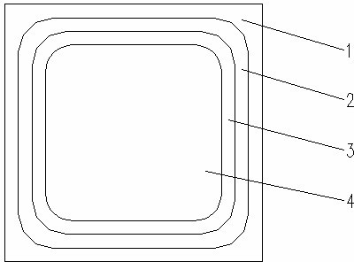
[0037] P + NN + The chip front section of the unidirectional high voltage transient voltage suppressor is as follows: TVS chip 1, mesa groove 2, glass layer 3, metal surface 4;

[0038] P + NP + Bi-directional high-voltage transient voltage suppressor, the front section of the chip is as follows: TVS chip 1, mesa groove 2, glass layer 3, metal surface 4;

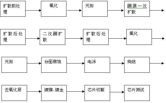
[0039] Such as figure 2 As shown, the chip process flow of the transient voltage suppressor TVS is as follows:

[0040] 1) Pre-diffusion treatment: chemically treat the sur...


PUM


Abstract

The invention relates to a high-voltage transient voltage suppressor chip and a production process. The high-voltage transient voltage suppressor chip is of a chip structure with increased auxiliary puncture diffusion junctions, a main junction of the chip enables the puncture voltage to reach 250V-400V, the puncture voltage of an auxiliary PN (positive-negative) junction designed in a region nearby a chip mesa trench is higher than that of the main junction so that the main junction is punctured firstly, leakage current is distributed in a main junction region, and the auxiliary junction region is not punctured. Therefore, the problems of high electricity leakage, low puncture voltage and easiness in damage when a high-voltage chip is produced by a single diffusion junction structure are solved, voltage resistance of a high-voltage transient voltage suppressor is improved, and anti-surge capacity and reliability of the transient voltage suppressor are enhanced.

Description

technical field [0001] The invention relates to the technical field of crystal diode chip production, in particular to a high-voltage transient voltage suppressor (TVS) chip and a production process. Background technique [0002] At present, the production process of transient voltage suppressor (TVS) chips in the semiconductor industry usually adopts the production process of double diffusion and single diffusion junction of paper source. There are problems in the existing technology: when a single diffusion junction is used in the production of transient voltage suppressor chips, if the reverse breakdown voltage reaches more than 250, when the chip breaks down, the surface electric field on the mesa is too high, causing the surface breakdown to precede the internal breakdown Breakdown, the breakdown current is concentrated near the table, which will increase the junction temperature of the table and easily cause damage to the chip. Therefore, the reverse breakdown voltage ...

Claims


Application Information

Patent Timeline
Patent Type & Authority Applications(China)
IPC IPC(8): H01L21/329H01L29/06H01L29/861
Inventor 薄勇王军明刘长蔚刘宁白树军王维卢凯刘振宇
Owner TIANJIN ZHONGHUAN SEMICON CO LTD
Why Eureka
Try Eureka