Method for forming semiconductor structure

A semiconductor and gate structure technology, applied in the field of semiconductor structure formation, can solve problems such as reducing the probability of carriers being trapped, and achieve the effect of suppressing hot electron effects and reducing interface defects

Inactive Publication Date: 2012-06-06
SEMICONDUCTOR MANUFACTURING INTERNATIONAL (BEIJING) CORP
View PDF9 Cites 10 Cited by
  • Summary
  • Abstract
  • Description
  • Claims
  • Application Information

AI Technical Summary

Problems solved by technology

However, these improvements do not involve reducing the probability of carriers being trapped in the oxide layer, that is, how to effective

Method used


Image

  • Method for forming semiconductor structure
  • Method for forming semiconductor structure
  • Method for forming semiconductor structure

Examples


Embodiment Construction

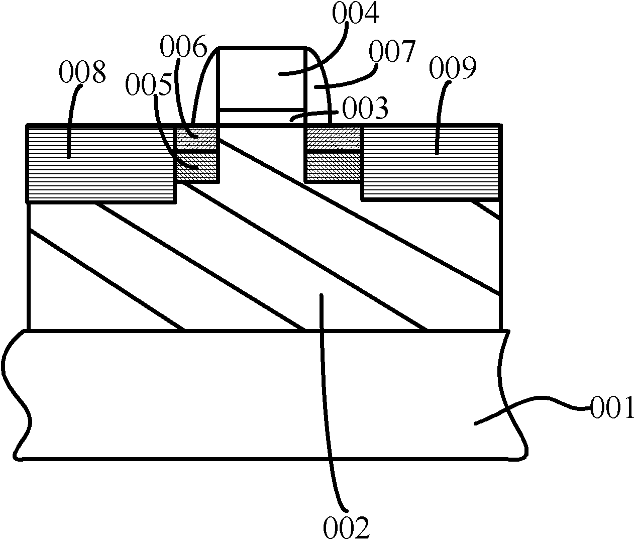
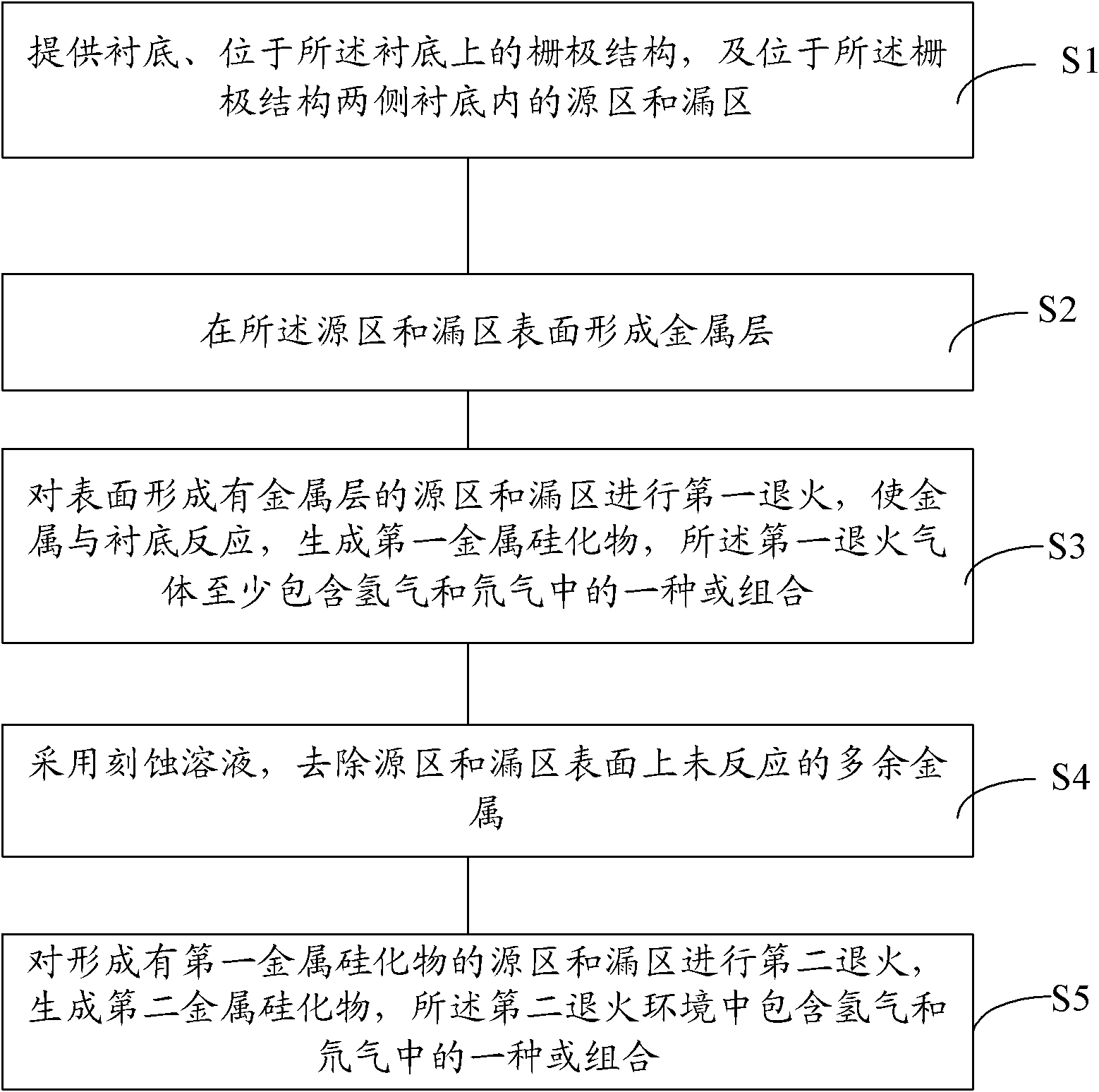
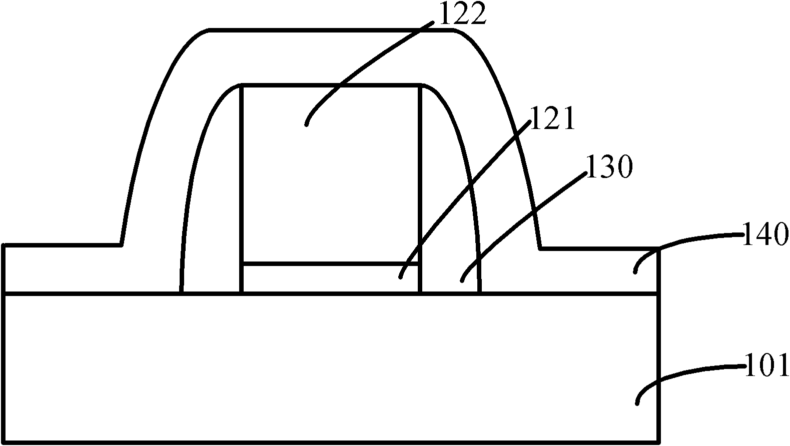
[0028] The invention provides a method for forming a semiconductor structure, including: providing a substrate, a gate structure on the substrate, and source regions and drain regions in the substrate on both sides of the gate structure; A metal layer is formed on the surface of the region and the drain region; an annealing process is performed on the source region and the drain region with the metal layer formed on the surface, and a metal silicide is formed in the source region and the drain region, wherein the annealing gas contains at least hydrogen and One or a combination of deuterium gases.

[0029] In the present invention, one or a combination of hydrogen and deuterium is added to any one or more annealing processes of the metal layer, so that the silicon dangling bonds in the substrate are bonded to one or a combination of hydrogen and deuterium combination, reduce the silicon dangling bonds located in the substrate, especially the silicon dangling bonds near the sub...


PUM


Abstract

The invention provides a method for forming a semiconductor structure, comprising the following steps of: providing a substrate, wherein the substrate is provided with a grid structure, a source region and a drain region positioned in the substrate at the two sides of the grid structure; forming metal layers on the surfaces of the source region and the drain region; and carrying out annealing process on the source region and the drain region forming the metal layers on the surfaces, and forming metal silicide in the source region and the drain region, wherein annealing gas at least comprises one or combination of hydrogen and deuterium. According to the method, by adding one or combination of the hydrogen and the deuterium into the annealing gas, silicon dangling bonds in the substrate are bonded with one or combination of the hydrogen and the deuterium, the silicon dangling bonds in the substrate are reduced, the interface defects nearby the substrate are reduced, and silicon-hydrogen bonds and silicon-deuterium bonds are stronger respectively, the cracking probability of the silicon-hydrogen bonds and the silicon-deuterium bonds is reduced under the external stress of the process environment, the interface defects nearby the substrate are further reduced, and the hot electron effect is restrained.

Description

technical field [0001] The invention relates to the field of semiconductor manufacturing, in particular to a method for forming a semiconductor structure. Background technique [0002] The main device in an integrated circuit, especially a VLSI, is a Metal Oxide Semiconductor (MOS for short). Since the invention of the integrated circuit, its performance and function have advanced by leaps and bounds, and the geometric size of the MOS device has been continuously reduced, and its feature size has entered the nanometer scale. [0003] In the process of scaling down the MOS device, the drain voltage does not decrease accordingly, which leads to the increase of the electric field in the channel region between the source and the drain. These electrons are called hot electrons, which are injected into the gate dielectric layer, thereby causing hot electron effect. This effect belongs to the small size effect of the device, which will cause gate electrode current and semiconduct...

Claims


Application Information

Patent Timeline
IPC IPC(8): H01L21/8232H01L21/335H01L21/324
Inventor 何永根
Owner SEMICONDUCTOR MANUFACTURING INTERNATIONAL (BEIJING) CORP
Why Eureka
Try Eureka