Method for embedding capacitor into PCB (printed circuit board) multilayer board
A technology of embedded capacitors and multi-layer boards, applied in the direction of multi-layer circuit manufacturing, etc., can solve the problems of broken capacitor materials, pollution of production lines, folding boards, etc., and achieve the effect of reducing production costs, reducing design requirements, and diversifying designs.
- Summary
- Abstract
- Description
- Claims
- Application Information
AI Technical Summary
Problems solved by technology
Method used
Image

Examples
Embodiment Construction
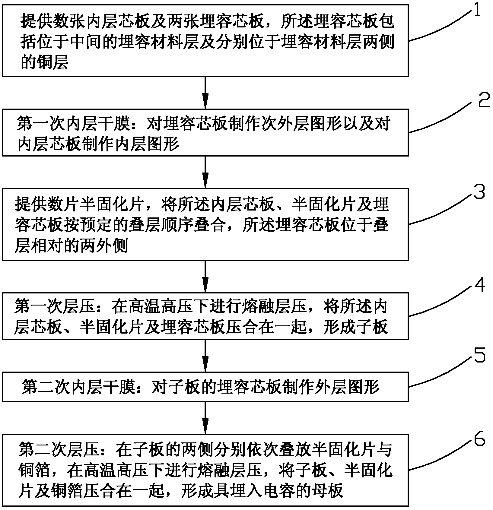
[0020] Such as Figure 1 to Figure 6 As shown, the method for embedding capacitors in the PCB multilayer board of the present invention comprises the following steps:
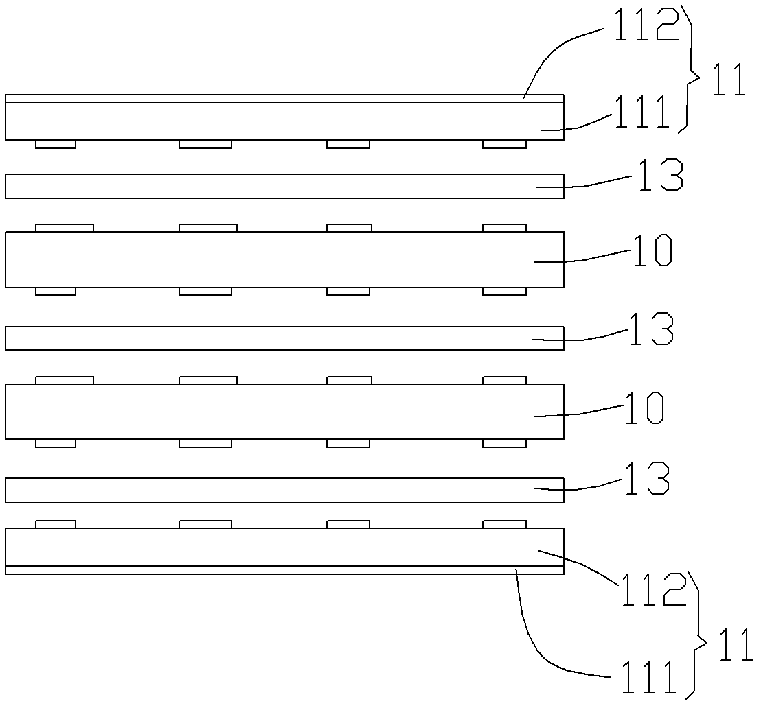
[0021] Step 1. Provide several inner core boards 10 and two embedding core boards 11, the embedding core boards 11 include an embedding material layer 111 in the middle and copper layers 112 respectively located on both sides of the embedding material layer 111 ;
[0022] Step 2, the first inner layer dry film: making the sub-outer layer graphics on the embedded core board 11 and making the inner layer graphics on the inner core board 10, including developing, etching, film stripping and other processes;
[0023] Step 3: Provide several pieces of prepreg 13, and stack the inner core board 10, prepreg 13 and embedded core board 11 according to a predetermined stacking sequence, and the embedded core board 11 is located on the two opposite sides of the stack;
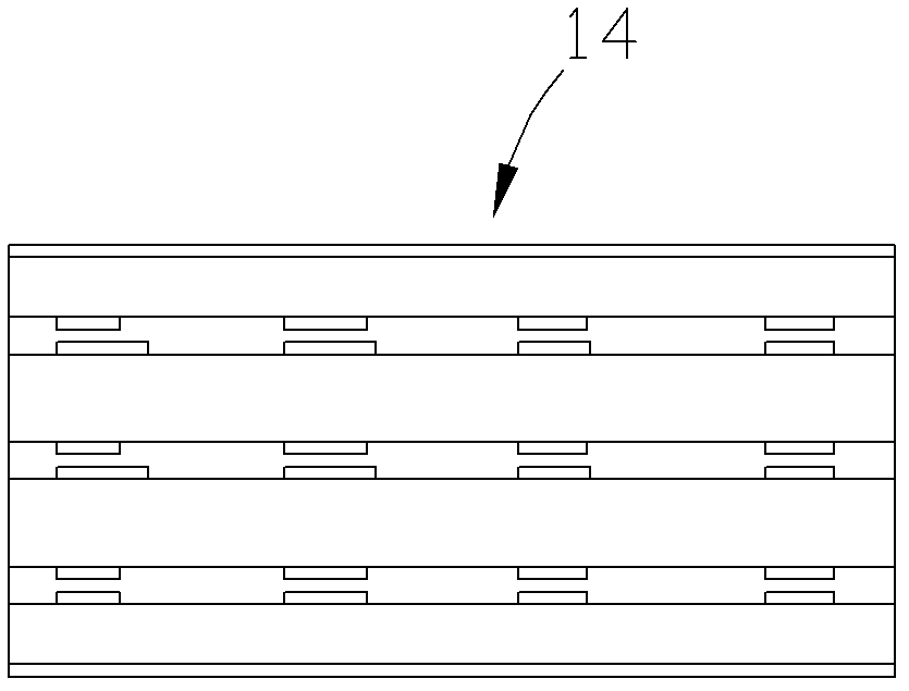
[0024] Step 4, the first lamination: melt laminati...
PUM
 Abstract
Description
Claims
Application Information
 - Generate Ideas
- Intellectual Property
- Life Sciences
- Materials
- Tech Scout
- Unparalleled Data Quality
- Higher Quality Content
- 60% Fewer Hallucinations
Browse by: Latest US Patents, China's latest patents, Technical Efficacy Thesaurus, Application Domain, Technology Topic, Popular Technical Reports.
© 2025 PatSnap. All rights reserved.Legal|Privacy policy|Modern Slavery Act Transparency Statement|Sitemap|About US| Contact US: help@patsnap.com