
Device and method for processing clock-domain-crossing asynchronous data, chip and operating method of chip

An asynchronous data, cross-clock domain technology, applied in the field of data processing, can solve the problems that affect the data processing accuracy of the data processing device, the clock signal has not been processed synchronously, and the clock signal has no timing relationship, so as to achieve good data processing accuracy , Work stability is good, the effect of improving work stability

Inactive Publication Date: 2012-06-20
ZHUHAI TIANWEI TECH DEV CO LTD
View PDF1 Cites 18 Cited by
  • Summary
  • Abstract
  • Description
  • Claims
  • Application Information

AI Technical Summary

Problems solved by technology

[0013] However, this method only uses the same clock signal to sample all data signals in the same clock domain, but there is no strict timing relationship between clock signals in different clock domains, that is, there is no strict timing relationship between clock signals in different clock domains. After the data is sampled by clock signals in different clock domains, there may still be inconsistencies in data synchronization, which affects the accuracy of data processing by the data processing device.

Method used


Image

  • Device and method for processing clock-domain-crossing asynchronous data, chip and operating method of chip
  • Device and method for processing clock-domain-crossing asynchronous data, chip and operating method of chip
  • Device and method for processing clock-domain-crossing asynchronous data, chip and operating method of chip

Examples


no. 1 example

[0041] The chip of this embodiment is an ink cartridge chip, which has a substrate, and one side of the substrate is provided with a plurality of electrical contacts as a communication unit for connecting with the electrical contacts of the inkjet printer. Of course, if wireless communication is performed between the inkjet printer and the consumable chip, the communication unit is an antenna for wireless communication. The other side of the substrate is provided with an electronic module connected with the electrical contacts, and the electronic module has a microcontroller and peripheral circuits of the microcontroller, including a filter circuit, a delay circuit, and the like.

[0042] The electronic module needs to process data in multiple clock domains, so a cross-clock domain asynchronous data processing device is provided. The electrical schematic diagram of the data processing device in this embodiment is as follows Image 6 shown.

[0043] The cross-clock domain asyn...

no. 2 example

[0055] This embodiment has a substrate on which electrical contacts and an electronic module are arranged. The electronic module has a microcontroller and peripheral circuits, and is also provided with a cross-clock domain asynchronous data processing device. The electrical schematic diagram of the device is shown in the figure below. Figure 8 shown.

[0056] The cross-clock domain asynchronous data processing device has a reference clock signal generating unit CLK, which generates a reference clock signal CK. The signal CK21 and the second clock signal CK22 of the second clock domain are sampled to obtain the first synchronization clock signal CK1B and the second synchronization clock signal CK2B, respectively.

[0057] The data sampling units DFF21 and DFF24 respectively sample the data D21 and the data D under the reference clock signal CK to obtain the sampled data signals D2A and D2B, and the data signal D2A is sampled by the data sampling unit DFF23 under the first sync...


PUM


Abstract

The invention provides a device and a method for processing clock-domain-crossing asynchronous data, a chip and an operating method of the chip. The device comprises a first data sampling unit, a second data sampling unit, a logical operation unit and a clock signal synchronization unit, wherein the first data sampling unit acquires data and obtains a first data signal in a first clock domain; the second data sampling unit acquires the data and obtains a second data signal in a second clock domain; the logical operation unit receives the first data signal and the second data signal and performs logical operation; the clock signal synchronization unit samples a first clock signal in the first clock domain and / or a second clock signal in the second clock domain to obtain a first synchronous clock signal and / or a second synchronous clock signal; and at least one of the first data sampling unit and the second data sampling unit acquires the data under the first synchronous clock signal and / or the second synchronous clock signal. The method comprises the following steps of: synchronizing clock signals in other clock domains by using a reference clock signal; and sampling the data. By the invention, data synchronism can be ensured, and the processing accuracy of the data is improved.

Description

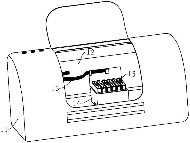
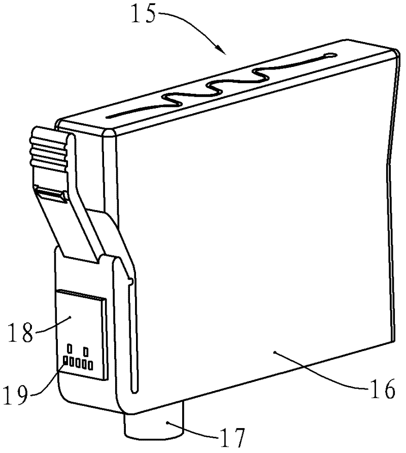
technical field [0001] The invention relates to the field of data processing, in particular to a cross-clock domain asynchronous data processing device, a data processing method of the device, a chip with the device and a working method of the chip. Background technique [0002] As a common office equipment, printers provide great convenience for modern office. Existing printers are divided into inkjet printers and laser printers. Inkjet printers use ink cartridges containing ink as consumable containers to spray ink on paper to form text or patterns that need to be printed on paper; laser printers use ink cartridges containing toner The toner cartridge is used as a consumable container to form text or patterns that need to be printed on the medium. [0003] see figure 1 , an existing color inkjet printer has a casing 11, figure 1 The inkjet printer is shown with the chassis 11 omitted. The machine core 12 of ink-jet printer is provided with in the casing 11, and is prov...

Claims


Application Information

Patent Timeline
IPC IPC(8): H03K19/173B41J2/175
Inventor 许兰
Owner ZHUHAI TIANWEI TECH DEV CO LTD
Learn More