Calibration method for photolithography line width test

A calibration method and technology of lithographic line width, which is applied in the direction of measuring devices, instruments, and wave/particle radiation, can solve problems such as the inability to guarantee the accuracy of lithographic line width testing, and achieve the effect of avoiding errors

Active Publication Date: 2016-03-02
CSMC TECH FAB2 CO LTD
View PDF5 Cites 0 Cited by
  • Summary
  • Abstract
  • Description
  • Claims
  • Application Information

AI Technical Summary

Problems solved by technology

However, the shape of the photoresist on the wafer is not consistent with the shape after etching, and the algorithm for calculating the line width is also different, and the line width test is greatly affected by these two factors, so the etching method is used. The scanning electron microscope calibrated after the wafer cannot guarantee the accuracy of the lithography line width test

Method used


Image

  • Calibration method for photolithography line width test
  • Calibration method for photolithography line width test

Examples


no. 1 approach

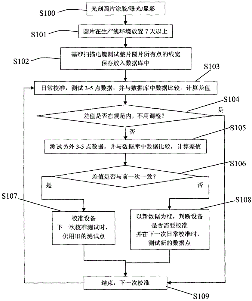
[0033] The first embodiment of the scanning electron microscope calibration of the present invention includes the following steps:

[0034] S100, gluing / exposure / development of the photolithography wafer;

[0035] S101. The wafer is placed in the production line environment for more than 7 days;

[0036] S102. The reference scanning electron microscope tests the line widths of all points on the entire wafer, and saves them in a database;

[0037] S103, daily calibration, test 3 to 5 points of data, compare with the data in the database, and calculate the difference;

[0038] S104. Determine whether the difference is within the specification and whether adjustment is required; if not, execute step S109, that is, end the current calibration, and proceed to the next calibration; if so, execute step 105;

[0039] S105. Test another 3 to 5 points of data, and compare with the data in the database, and calculate the difference;

[0040] S106, judging whether the difference is con...

no. 2 approach

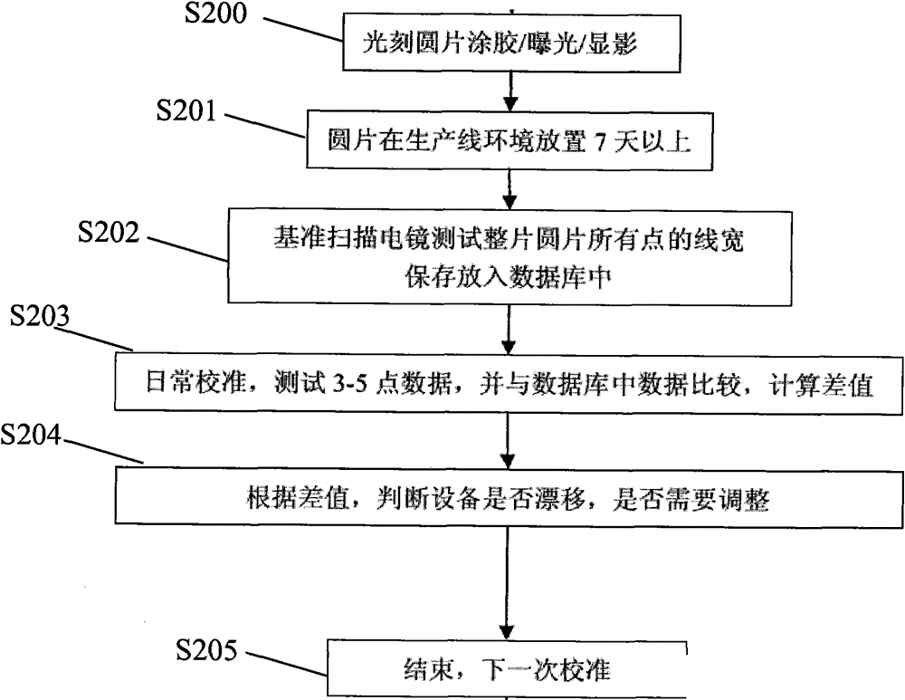
[0045] The second embodiment of the scanning electron microscope calibration of the present invention includes the following steps:

[0046] S200, gluing / exposure / development of photolithography wafer;

[0047] S201. The wafer is placed in the production line environment for more than 7 days;

[0048] S202. The reference scanning electron microscope tests the line widths of all points on the entire wafer, and saves them in a database;

[0049] S203, daily calibration, test 3 to 5 points of data, compare with the data in the database, and calculate the difference;

[0050] S204. According to the difference, determine whether the device drifts and whether adjustment is required; if adjustment is not required, proceed to S205;

[0051] S205. End the current calibration and start the next calibration, that is, repeat steps S203 and S204.

[0052] The test points for each calibration in the above process are different, and the appearance of the test points is not damaged, which ...


PUM


Abstract

The invention provides a photolithographic line width test calibration method which comprises the following steps: S100, carrying out exposure on a photolithographic wafer; S101, standing the wafer subjected to exposure for several days; S102, testing the line widths of all points of the whole wafer by using a reference scanning electron microscope, and storing the line widths into a database; S103, carrying out daily calibration, testing the data of the first group of test points on the wafer, and comparing the tested data with data in the database so as to calculate a first difference value; and S104, judging whether the first difference value is within a standard and whether the first difference value needs to be adjusted; if not, completing the current calibration. Compared with the prior art, the method disclosed by the invention has the advantages that an error caused by the difference between the appearance of an etched wafer or a standard sample provided by a manufacturer and the appearance of a photolithographic sample is avoided during the measurement on photolithographic line width; in addition, calibration is not affected by appearance damage caused when electron beams bombard samples.

Description

technical field [0001] The invention relates to a method for testing and calibrating photolithographic line width, and relates to a semiconductor production process. Background technique [0002] The line width test (CD, Critical Dimension) in integrated circuit production is generally measured by optical microscope and scanning electron microscope. In advanced semiconductor processes, line width dimensions are getting smaller and smaller, so higher-resolution scanning electron microscopes are mainly used for testing. [0003] The basic working principle of the scanning electron microscope is that the electrons are emitted by the electron gun, accelerated under the electric field, focused by the electromagnetic lens, and become a very fine electron beam, which is scanned on the surface of the sample under the action of the scanning coil to stimulate various physical signals. Intensity varies with surface features. The signal is detected by a detector, amplified, and the mo...

Claims


Application Information

Patent Timeline
Patent Type & Authority Patents(China)
IPC IPC(8): G01B15/00
Inventor 黄玮
Owner CSMC TECH FAB2 CO LTD
Why Eureka
Try Eureka