BIST (Built-in Self-test) automatic test circuit and test method aiming at PHY (Physical Layer) high-speed interface circuit

A high-speed interface and automatic test technology, applied in electrical digital data processing, error detection/correction, instruments, etc., can solve problems such as high test cost, complexity, and difficulty in capturing interface output signals, and achieve control of test cost and hardware overhead Effects of smallness, reduced complexity and test time

Inactive Publication Date: 2012-07-11
北京国睿中数科技股份有限公司
View PDF3 Cites 13 Cited by
  • Summary
  • Abstract
  • Description
  • Claims
  • Application Information

AI Technical Summary

Problems solved by technology

The reason for this is that on the one hand, the high-speed characteristics of these interface circuits make it very difficult to capture the output signal of the interface on the ATE test machine, and upgrading or replacing existing test equipment means huge economic On the other hand, due to the independence and uncontrollability of these fully customized interface modules, the related tests have become a kind of black box test, which cannot be improved by inserting scan chains and other commonly used testable design techniques. control and observability, so that the traditional test method is only available for direct observation of its output at the peripheral interface of the circuit, and this method also has great complexity and high test cost

Method used


Image

  • BIST (Built-in Self-test) automatic test circuit and test method aiming at PHY (Physical Layer) high-speed interface circuit
  • BIST (Built-in Self-test) automatic test circuit and test method aiming at PHY (Physical Layer) high-speed interface circuit
  • BIST (Built-in Self-test) automatic test circuit and test method aiming at PHY (Physical Layer) high-speed interface circuit

Examples


Embodiment Construction

[0035] Certain terms are used throughout this document to refer to particular system components. As those skilled in the art will recognize, the same components may often be referred to by different names, and thus this document does not intend to distinguish between those components that differ only in name but not in function. In this document, the terms "including", "comprising" and "having" are used in an open form and should therefore be construed to mean "including but not limited to...".

[0036] The present invention will be further described in detail below in combination with preferred embodiments of the present invention.

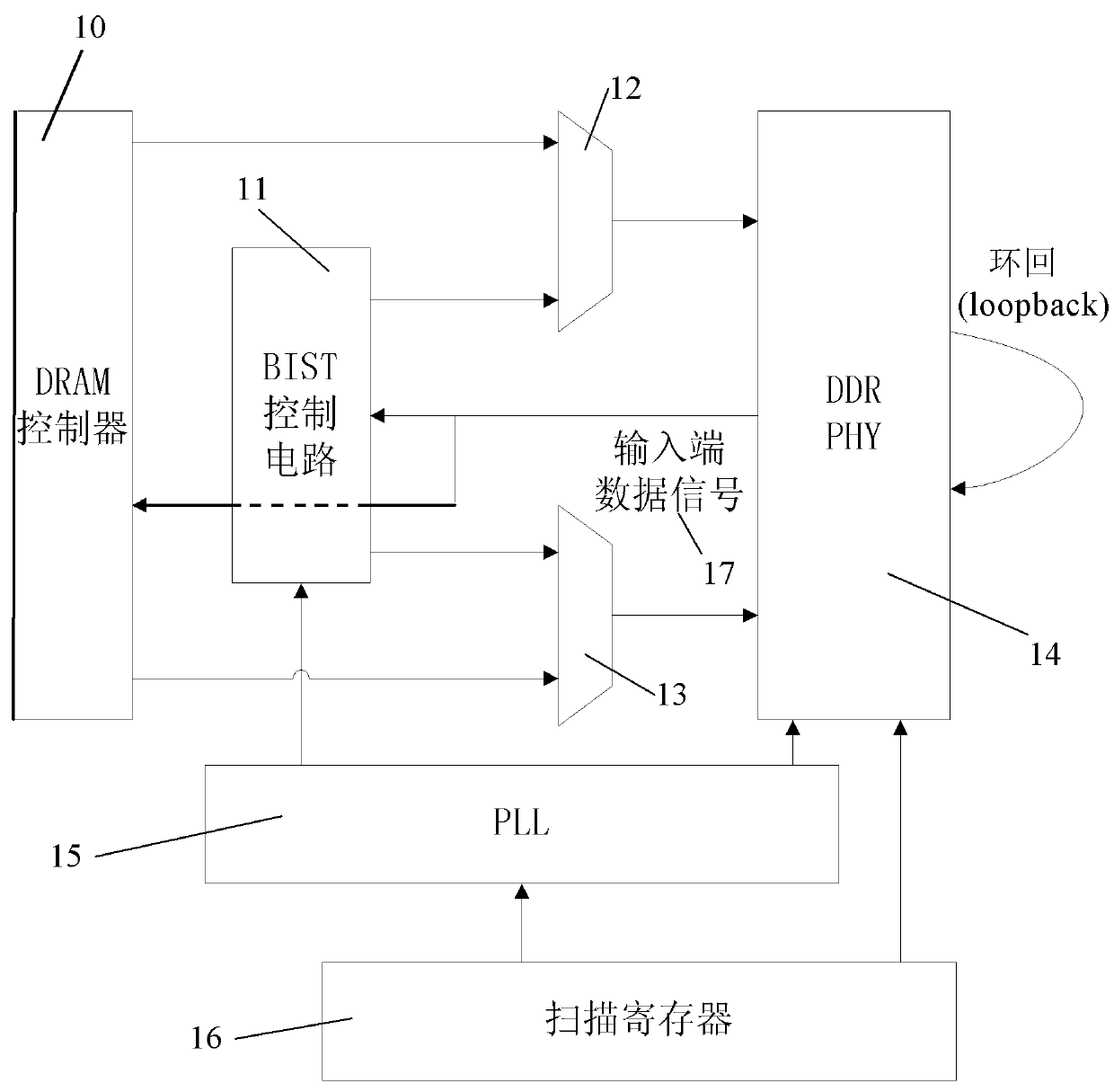
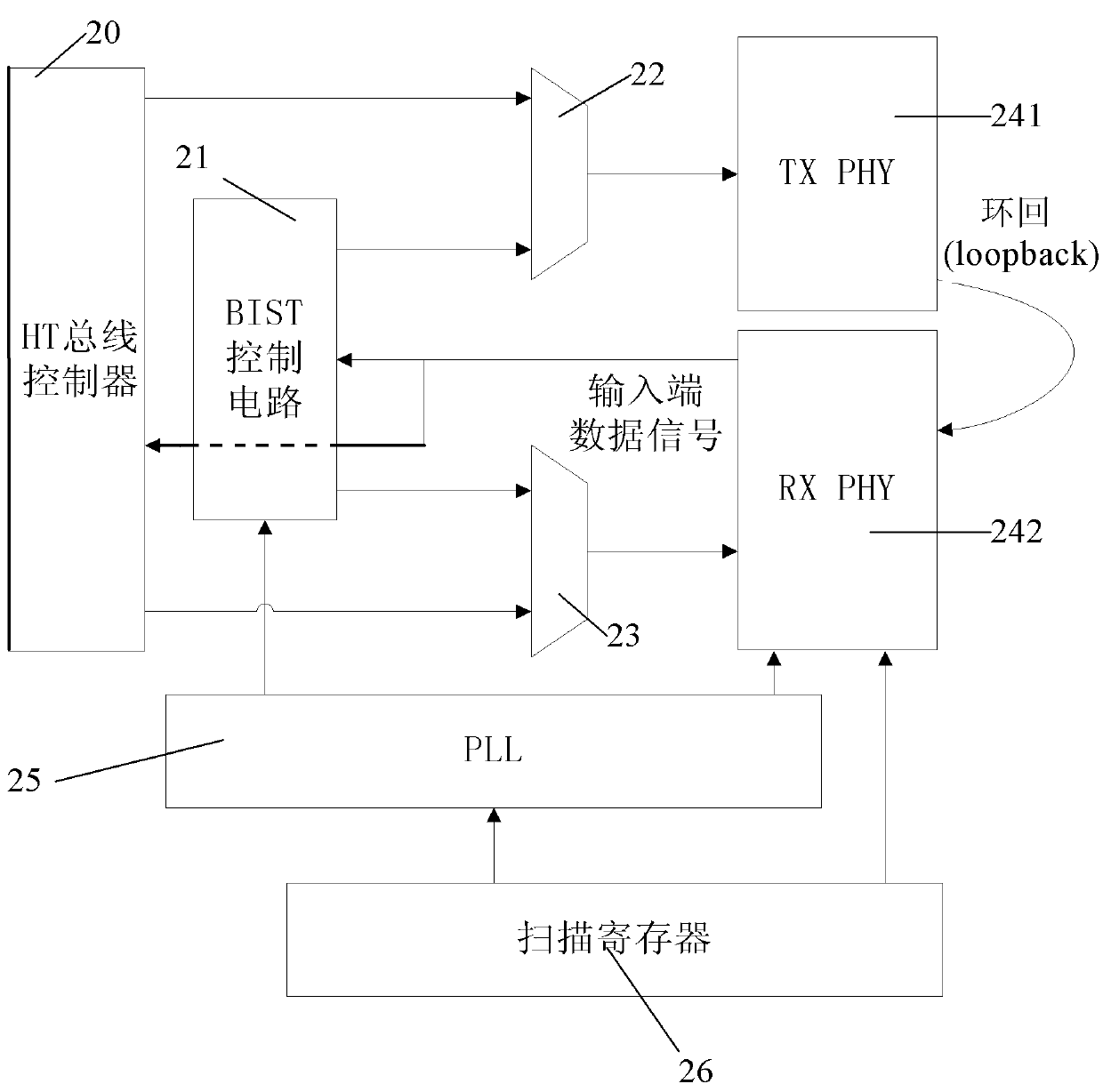
[0037] As mentioned above, the present invention aims to provide a BIST automatic testing circuit and testing method for PHY high-speed interface circuits.

[0038]BIST automatic test is to implant the built-in self-test circuit in the circuit when designing the circuit (that is, integrate the built-in self-test circuit and the functional circui...


PUM


Abstract

The invention discloses a BIST (Built-in Self-test) automatic test circuit and a test method aiming at a PHY (Physical Layer) high-speed interface circuit. The test circuit comprises a BIST control circuit, an analog circuit parameter control scan chain, two selectors and a test result output circuit, wherein the BIST control circuit has the functions of automatically generating control signals and data and comparing results. The test method comprises the following steps of: (1) entering into an ATPG (Automatic Test Pattern Generation) scan mode; (2) configuring the parameter of the PHY high-speed interface circuit and the parameter of a PLL (Phase Locked Loop) circuit through the scan chain; (3) entering into a PHYBIST test mode; (4) starting to automatically generate a test vector, and inputting a measurement vector to the PHY high-speed interface circuit; (5) returning the data in a built-in loopback way, and comparing the correctness of the returned data; and (6) outputting a test result. According to the test circuit disclosed by the invention, the PHY high-speed interface circuit can be effectively tested under an actual speed mode, the cost of hardware is low, the control is simple, and the complex degree and the test time of the test vector used by ATE (Automatic Test Equipment) are reduced.

Description

technical field [0001] The present invention relates to the field of automatic testing, in particular to the field of testing methodology for ATE (Automatic Test Equipment, i.e. automated testing equipment) testing machines, more specifically to a high-speed PHY (Physical Layer, i.e. physical layer) The BIST (Built-in Self-Test) test circuit and test method of the interface circuit. Background technique [0002] Integrated circuit testing is of great significance to the development of integrated circuits. It is not only an important basis to guide product design, production and use, but also an effective measure to improve product quality and reliability and conduct total quality management. [0003] With the development of the field of integrated circuits, some interface circuits are gradually replaced by fully customized high-speed analog circuits (PHY) due to their high operating speed. At present, the testing of these PHY high-speed interface circuits has unprecedented ...

Claims


Application Information

Patent Timeline
Patent Type & Authority Applications(China)
IPC IPC(8): G06F11/267
Inventor 毛鲁丁
Owner 北京国睿中数科技股份有限公司
Why Eureka
Try Eureka