Method for manufacturing metal oxide semiconductor (MOS) tube

A technology of semiconductor tubes and manufacturing methods, which is applied in the field of metal oxide semiconductor tubes, and can solve the problems of uneven saturation current of MOS tubes, hindering the etching of ONO sidewall layers, and large differences in the characteristic dimensions of ONO sidewall layers.

Inactive Publication Date: 2012-07-11
SEMICON MFG INT (SHANGHAI) CORP +1
View PDF5 Cites 2 Cited by
  • Summary
  • Abstract
  • Description
  • Claims
  • Application Information

AI Technical Summary

Problems solved by technology

However, since the above two-step etching uses a gas with a high etching selectivity ratio, a large amount of organic polymers (polymers) will be produced during the etching process, and these polymers are attached to the ONO sidewall layer during the formation process. Hinder the etching of the ONO sidewall layer, and these polymers greatly change the etching rate of the ONO sidewall layer formed by etching, so the characteristic size of the ONO sidewall layer of each MOS tube formed will vary greatly, ONO The characteristic dimensions of the sidewall layer are as figure 1 The range indicated by the two-way arrow in
The characteristic size of the ONO sidewall layer of the MOS tube is not uniform, which means that the saturation current of the MOS tube is not uniform

Method used


Image

  • Method for manufacturing metal oxide semiconductor (MOS) tube
  • Method for manufacturing metal oxide semiconductor (MOS) tube
  • Method for manufacturing metal oxide semiconductor (MOS) tube

Examples


Embodiment Construction

[0033] In order to make the object, technical solution, and advantages of the present invention clearer, the present invention will be further described in detail below with reference to the accompanying drawings and examples.

[0034] The present invention has been described in detail using schematic diagrams. When describing the embodiments of the present invention in detail, for the convenience of explanation, the schematic diagram showing the structure will not be partially enlarged according to the general scale, which should not be used as a limitation of the present invention. In addition, in actual production In , the three-dimensional space dimensions of length, width and depth should be included.

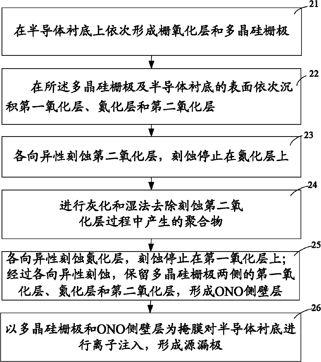
[0035] The manufacturing method of MOS tube of the present invention comprises the following steps, and the schematic flow chart is as figure 2 shown.

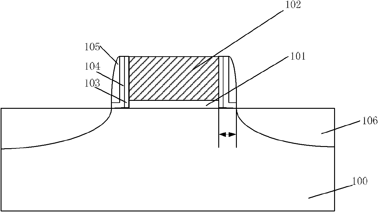
[0036] Step 21, sequentially forming a gate oxide layer 101 and a polysilicon gate 102 on the semiconductor substrate ...


PUM

PropertyMeasurementUnit
thicknessaaaaaaaaaa
thicknessaaaaaaaaaa
thicknessaaaaaaaaaa

Abstract

The invention provides a method for manufacturing a metal oxide semiconductor (MOS) tube. The method comprises the following steps of: sequentially forming a grid oxide layer and a polysilicon grid on a semiconductor substrate; sequentially depositing a first oxide layer, a nitrided layer and a second oxide layer on the surfaces of the polysilicon grid and the semiconductor substrate; anisotropically etching the second oxide layer, and stopping etching on the nitrided layer; performing ashing and a wet process to remove polymers during etching of the second oxide layer; anisotropically etching the nitrided layer, and stopping etching on the first oxide layer; retaining the first oxide layer, the nitrided layer and the second oxide layer on two sides of the polysilicon grid through anisotropic etching, and forming an oxide-nitride-oxide (ONO) side wall layer; and performing ion injection on the semiconductor substrate by taking the polysilicon grid and the ONO side wall layer as masks, and forming a source and a drain. By adopting the method provided by the invention, the uniformity of a critical dimension of the ONO side wall layer of the MOS tube can be improved.

Description

technical field [0001] The invention relates to semiconductor device manufacturing technology, in particular to a method for manufacturing a metal oxide semiconductor (MOS) tube. Background technique [0002] At present, in the manufacturing process of semiconductor devices, P-type metal-oxide-semiconductor (PMOS) tubes, NMOS tubes, or complementary metal-oxide-semiconductor (Complementary Metal-Oxide-Semiconductor, CMOS) tubes composed of PMOS tubes and NMOS tubes Tubes become the basic devices that make up chips. [0003] The manufacturing method of MOS tube in the prior art comprises the following steps: [0004] Step 11, sequentially forming a gate oxide layer 101 and a polysilicon gate 102 on the semiconductor substrate 100; [0005] Specifically, a gate oxide layer and a polysilicon layer are sequentially grown on the semiconductor substrate 100 , and then the polysilicon layer and the gate oxide layer are etched to form a gate oxide layer 101 and a polysilicon gate ...

Claims


Application Information

Patent Timeline
Patent Type & Authority Applications(China)
IPC IPC(8): H01L21/336H01L21/311
Inventor 唐兆云
Owner SEMICON MFG INT (SHANGHAI) CORP
Why Eureka
Try Eureka