

Patterned substrate for aluminum nitride (AlN) crystal growth
A technology for patterning substrates and crystal growth, applied in crystal growth, single crystal growth, single crystal growth and other directions, can solve the problems that SiC seed crystal affects the quality of AlN crystal and the high cost of AlN seed crystal, and achieves large diameter and defects. low density effect
- Summary
- Abstract
- Description
- Claims
- Application Information
AI Technical Summary
Problems solved by technology
Method used
Image

Examples
specific Embodiment approach 1
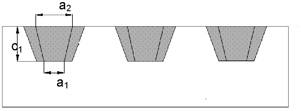
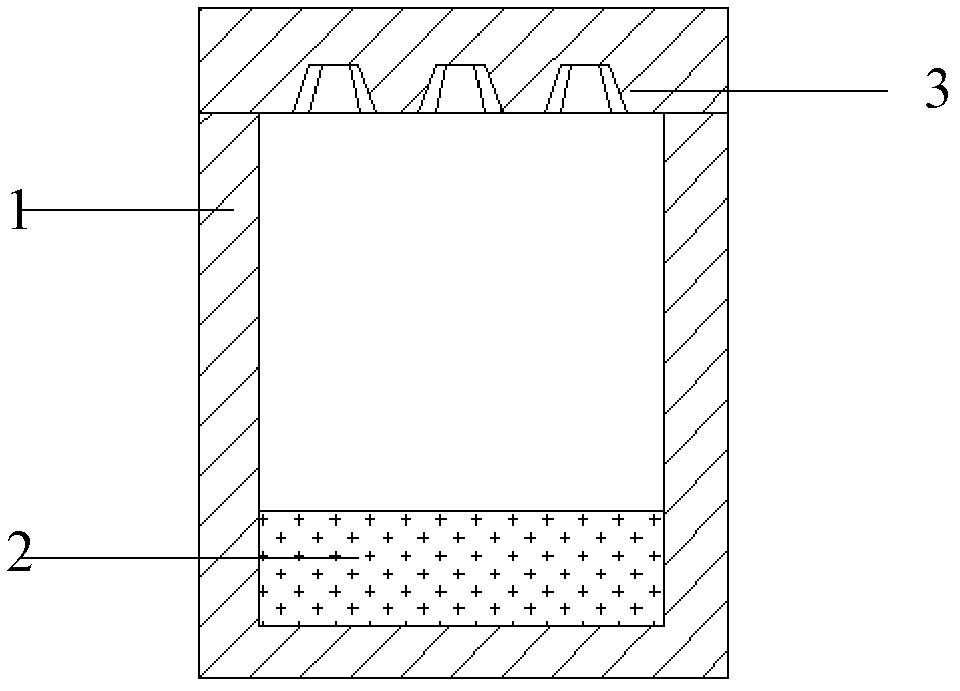
[0018] Specific Embodiment 1: This embodiment is a patterned substrate for AlN crystal growth. The patterned substrate for AlN crystal growth is to embed evenly arranged graphic units on the substrate, and the shape of the graphic units is a regular hexagonal truss , side length is a 2 The upper bottom surface of is on the plane where the substrate surface is located, and the side length of the lower bottom surface is a 1 , the height of the graphics unit is c 1 , where a 1 =n 1 a,c 1 =n 1 c, a 2 =n 2 a 1 , a and c are the unit cell parameters of the hexagonal AlN crystal, 01 ≤15×10 7 , 12 ≤3.
[0019] The side length a of the bottom surface of the graphic unit described in this embodiment1 and height c 1 n is the corresponding AlN unit cell parameter 1 times, 01 ≤15×10 7 , n 1 The value of includes but not limited to (0, 15×10 7 ] an integer in the interval.
[0020] In this embodiment n 2 The value of includes but not limited to integers in the interval (1,...
specific Embodiment approach 2
[0024] Specific embodiment two: the difference between this embodiment and specific embodiment one is n 1 is an integer, n 2 is an integer. Other parameters are the same as in the first embodiment.
[0025] In this embodiment n 1 is (0, 15×10 7 ) an integer in the interval, i.e. the side length a of the bottom surface of the graphic unit 1 and height c 1 is an integer multiple of the corresponding AlN unit cell parameter (n 1 times), the side length of the upper bottom surface of the graphic unit a 2 is an integer multiple of the AlN unit cell parameter a (n 1 n 2 times).
[0026] with n 1 , n 2 When it is a non-integer multiple, when n 1 , n 2 The pattern unit when is an integer will be more beneficial to control the growth process of the AlN crystal, which is shown in: due to the limitation on the size, when the AlN single crystal is deposited at the unit pattern, it is more likely to form several integer AlN unit cells, while The unit cells will also be arrang...
specific Embodiment approach 3
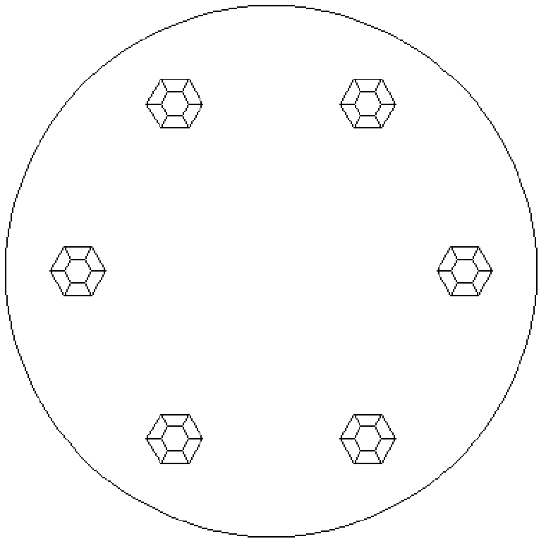
[0027] Embodiment 3: The difference between this embodiment and Embodiment 1 or 2 is that the patterned substrates for AlN crystal growth are evenly arranged in one of regular hexagons, rhombuses, and regular triangles, or a combination of several of them. graphics unit. Other parameters are the same as those in Embodiment 1 or Embodiment 2.
[0028] In this embodiment, a schematic diagram of a patterned substrate for AlN crystal growth with patterned units evenly arranged in a regular hexagonal manner is as follows image 3 shown.
[0029] In this embodiment, a schematic diagram of a patterned substrate for AlN crystal growth with pattern units evenly arranged in a rhombus manner is as follows Figure 4 shown.
[0030] In this embodiment, a schematic diagram of a patterned substrate on which patterned units are evenly arranged in an equilateral triangle pattern for AlN crystal growth is as follows Figure 5 shown.
[0031] In this embodiment, a schematic diagram of a pat...
PUM
 Abstract
Description
Claims
Application Information