Printed circuit board
A technology for printed circuit boards and substrates, applied in the direction of printed circuit components, etc., can solve the problems of increasing PCB manufacturing costs, small trace width, etc., to enhance stability, improve power supply and reflow capabilities, and reduce the number of layers used in PCBs Effect
- Summary
- Abstract
- Description
- Claims
- Application Information
AI Technical Summary
Problems solved by technology
Method used
Image

Examples
Embodiment Construction
[0016] According to the resistance formula: R = ρ l A
[0017] Among them, ρ is the resistivity, l is the length of the wire, A is the cross-sectional area,
[0018] In the case of constant resistivity and thickness, the trace area should be increased as much as possible.
[0019] In addition, according to the ideal return path ground bounce voltage drop formula:
[0020] Among them, V gb is the ground bounce voltage, L total is the total return path inductance, L b is the local self-inductance, L ab is the local mutual inductance,
[0021] It can be deduced that when the signal edge change rate cannot be reduced and the number of layers of the PCB return path cannot be reduced, the trace width should be increased as much as possible.
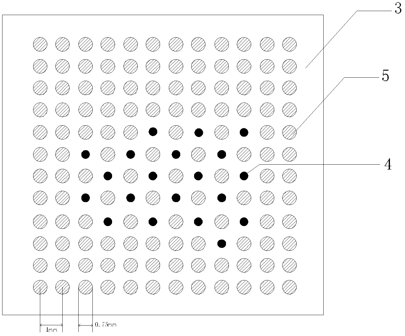
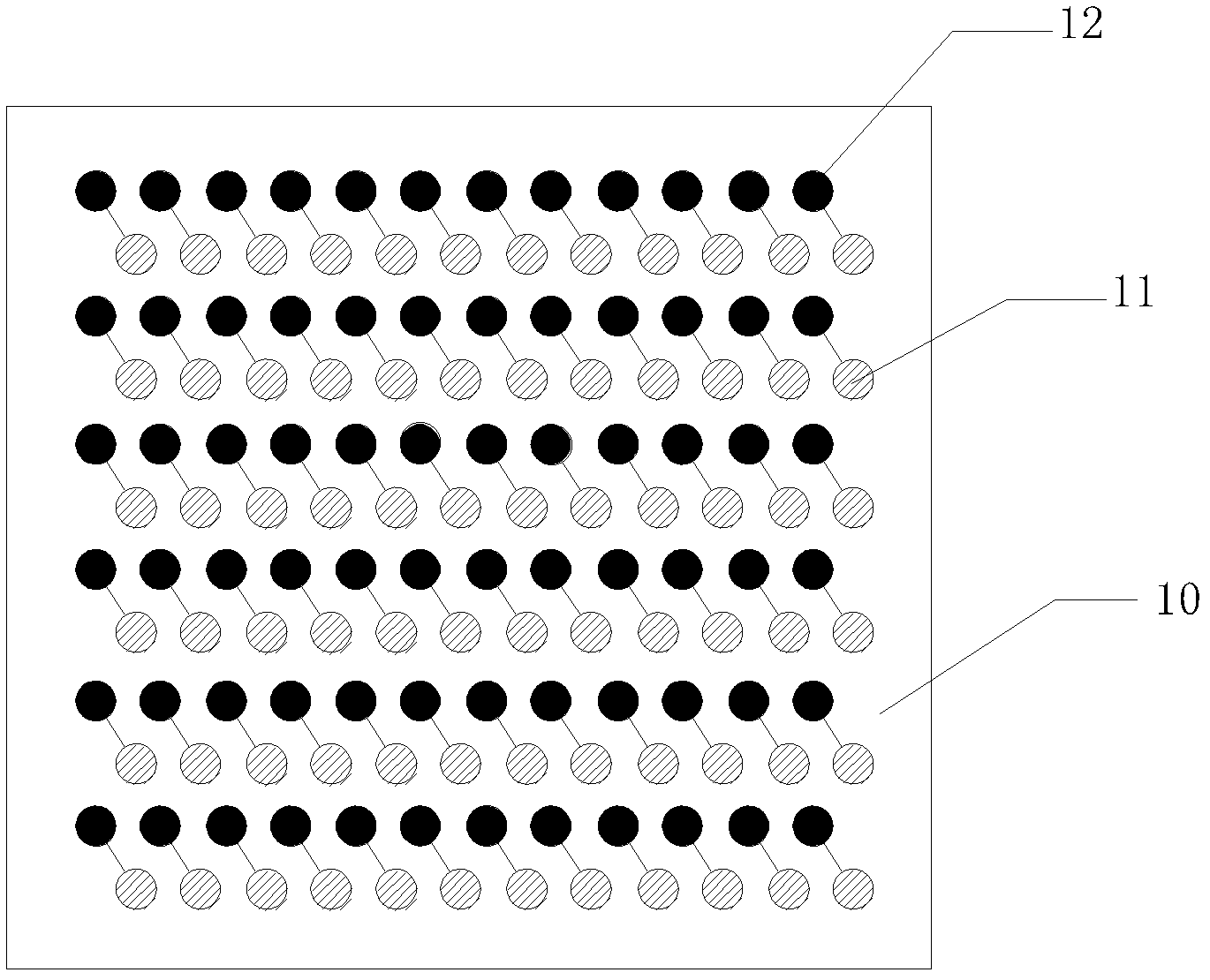
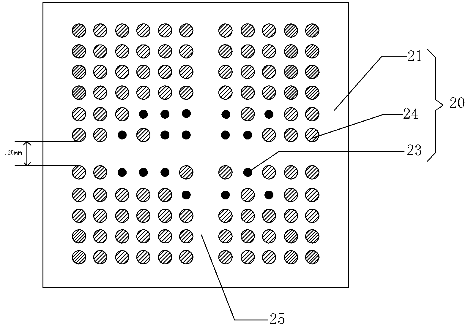
[0022] The PCB board of the present invention includes a surface layer board 10 , a power plane layer board 20 , a ground layer board 30 and a bottom layer boar...
PUM
| Property | Measurement | Unit |
|---|---|---|
| Width | aaaaa | aaaaa |
Abstract
Description
Claims
Application Information
 - R&D Engineer
- R&D Manager
- IP Professional
- Industry Leading Data Capabilities
- Powerful AI technology
- Patent DNA Extraction
Browse by: Latest US Patents, China's latest patents, Technical Efficacy Thesaurus, Application Domain, Technology Topic.
© 2024 PatSnap. All rights reserved.Legal|Privacy policy|Modern Slavery Act Transparency Statement|Sitemap