Metal-oxide semiconductor field effect transistor integrated with capacitor

A technology of field effect transistors and capacitors, which is applied in the field of metal oxide semiconductor field effect transistors and its preparation, and can solve problems such as chip functional failure and wafer particle fragmentation

Active Publication Date: 2012-07-25
重庆万国半导体科技有限公司
View PDF6 Cites 2 Cited by
  • Summary
  • Abstract
  • Description
  • Claims
  • Application Information

AI Technical Summary

Problems solved by technology

Furthermore, in the process steps of die attaching thin wafer particles to a lead frame (Leadframe) or a substrate (Substrate) such as a PCB, it is easy to cause wafer particle fragmentation (Die Crack) so that Chips fail functionally, and that's not what we want

Method used


Image

  • Metal-oxide semiconductor field effect transistor integrated with capacitor
  • Metal-oxide semiconductor field effect transistor integrated with capacitor
  • Metal-oxide semiconductor field effect transistor integrated with capacitor

Examples


Embodiment 1

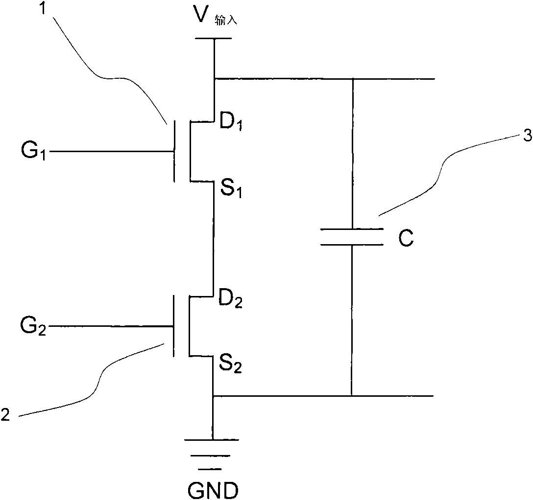
[0052] see Figure 2A (Schematic diagram of three-dimensional structure), 2B-2F (Schematic plan view of the level where each layer of capacitive plates are located correspondingly from bottom to top in the schematic diagram of three-dimensional structure), on a silicon chip substrate 110 top surface is provided with The gate metal layer 120 (referred to as the second electrode metal layer) of the MOS field effect transistor 100 gate electrode (referred to as the second electrode) constituting the low side (LowSide), and the source electrode constituting the MOS field effect transistor 100 (referred to as the second electrode) The source metal layer 130 (referred to as the first electrode metal layer), the source metal layer 130 includes an extension structure 135 . The drain (not shown) of the MOS field effect transistor 100 is formed on the bottom surface of the silicon substrate 110, and the source (not shown) and gate (not shown) of the MOS field effect transistor 100 are f...

Embodiment 2

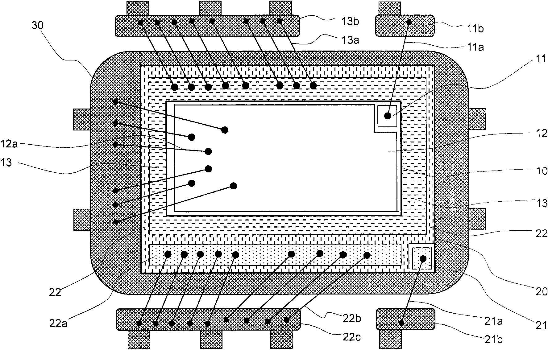
[0057] see Figure 3A (Schematic diagram of three-dimensional structure), 3B-3F (Schematic plan view of the level where each layer of capacitor plate is located correspondingly from bottom to top in the schematic diagram of three-dimensional structure), on a silicon chip substrate 210 top surface is provided with The gate metal layer 220 (referred to as the second electrode metal layer) of the MOS field effect transistor 200 gate electrode (referred to as the second electrode) constituting the low side (LowSide), and the source electrode constituting the MOS field effect transistor 200 (referred to as the second electrode) The source metal layer 230 (referred to as the first electrode metal layer), the source metal layer 230 includes an extension structure 235 . The drain (not shown) of the MOS field effect transistor 200 is formed on the bottom surface of the silicon substrate at 210, and the source (not shown) and the gate (not shown) of the MOS field effect transistor 200 a...

Embodiment 3

[0062] In fact, with the continuous improvement of the dielectric constant of the dielectric used in the capacitor, the above-mentioned embodiment is slightly cumbersome, and the general capacitor does not need so many multi-layer capacitor plates as in the above-mentioned embodiment 1 or 2, as a further improvement of the above-mentioned embodiment Improvement, the following content will provide a more concise implementation.

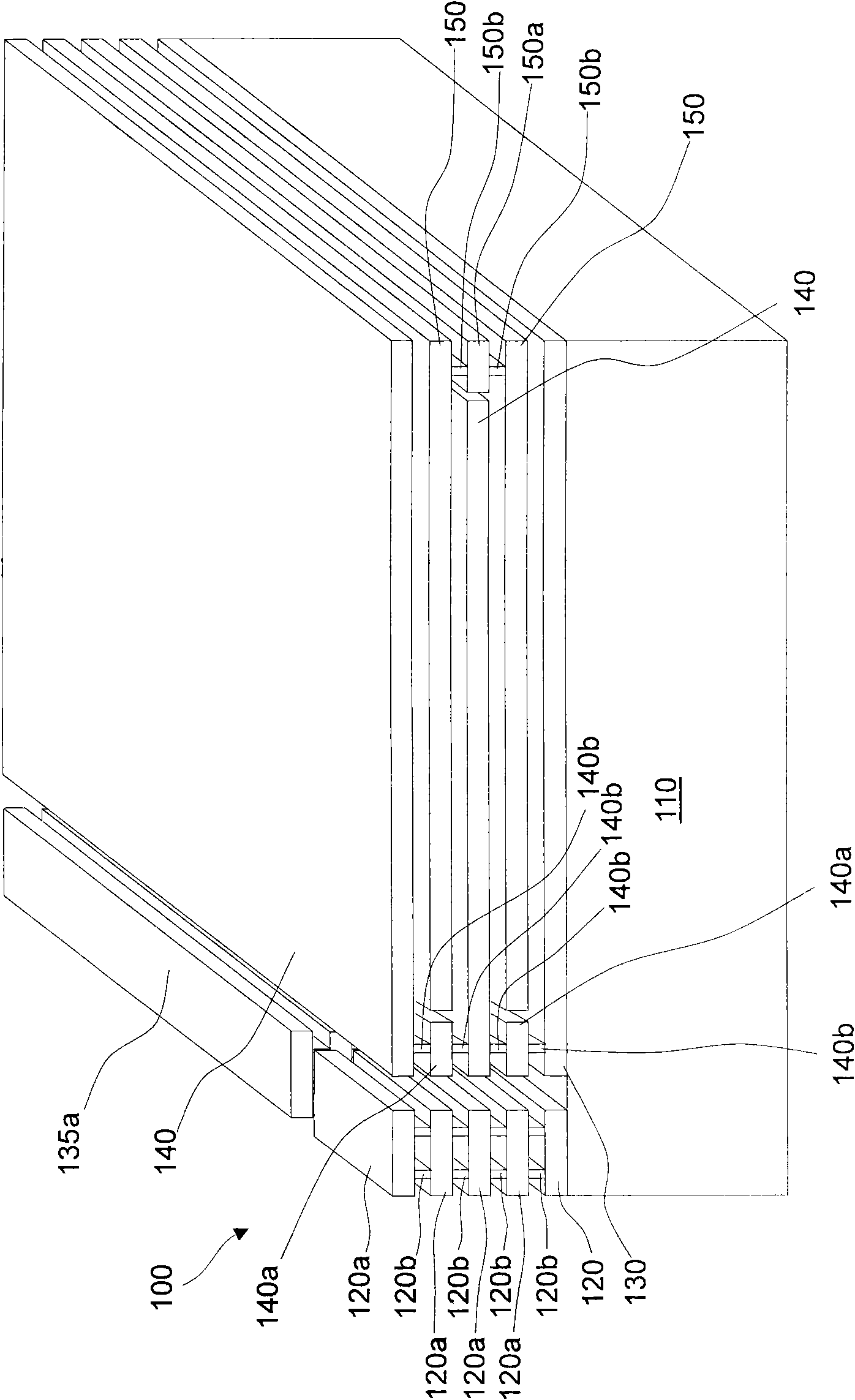
[0063] see Figure 4A(Schematic diagram of three-dimensional structure), 4B-4E (Schematic diagram of the planar view of the level where each layer of capacitor plate is located correspondingly from bottom to top in the schematic diagram of three-dimensional structure), the MOS field effect transistor 300 is integrated with a bypass capacitor, Wherein: the gate metal layer 320 (referred to as the second electrode metal) of the gate electrode (referred to as the second electrode) of the MOS field effect transistor 300 (referred to as the second electrode...


PUM


Abstract

The invention relates to a metal-oxide semiconductor field effect transistor and particularly relates to the metal-oxide semiconductor field effect transistor integrated with a capacitor, and a manufacturing method of the metal-oxide semiconductor field effect transistor integrated with the capacitor. According to the invention, the capacitor is directly integrated on the metal-oxide semiconductor field effect transistor, so that the mode that the metal-oxide semiconductor field effect transistor tube is connected with an external capacitor by a bonding alloy wire is replaced, and further the discrete inductance in the line connection can be eliminated greatly. Due to the existence of a capacitance pole plate and a dielectric layer, the thickness of a silicon substrate and the mechanical strength of the silicon substrate are improved, and according to the advantages, the silicon substrate can be thinned so as to obtain low resistance of the metal-oxide semiconductor field effect transistor.

Description

technical field [0001] The present invention generally relates to a metal-oxide-semiconductor field-effect transistor, and more precisely, the present invention relates to a metal-oxide-semiconductor field-effect transistor integrated with a capacitor and a manufacturing method thereof. Background technique [0002] In power devices, a bypass capacitor is usually connected between the power supply of DC-DC power switching and ground (GND). There is pulsation in the current of the working circuit, such as the synchronous frequency of the digital circuit, which is easy to cause the pulsation of the power supply voltage, which is a kind of AC noise, and the small-capacity non-polar capacitor can bypass this noise to the ground; The continuous reduction requires DC-DC converters to have low voltage and high current output. In DC-DC converters, a capacitor is often used as a filter capacitor. In order to improve stability, the above capacitor is very important to improve the perf...

Claims


Application Information

Patent Timeline
Patent Type & Authority Applications(China)
IPC IPC(8): H01L27/06H01L21/70
Inventor 薛彦迅安荷·叭剌哈姆扎·耶尔马兹鲁军
Owner 重庆万国半导体科技有限公司
Why Eureka
Try Eureka