Manufacturing method for semiconductor devices with super junction structures

A manufacturing method and semiconductor technology, applied in the direction of semiconductor/solid-state device manufacturing, electrical components, circuits, etc., can solve the problem that the part filled with insulating material cannot be used as a current flow path, the chip area cannot be fully utilized, and the on-resistance of the device can be reduced. , to achieve the effect of simple and easy manufacturing process, reducing on-resistance, and increasing the current flow path

Inactive Publication Date: 2012-08-01
WUXI NCE POWER
View PDF7 Cites 9 Cited by
  • Summary
  • Abstract
  • Description
  • Claims
  • Application Information

AI Technical Summary

Problems solved by technology

[0006] Chinese patent 200680013510.6 mentions a method of using oblique angle implantation to realize P columns in a super junction structure. Although it is possible to produce relatively narrow P columns, since the deep trenches are filled with insulating materials after implantation, the filling of insulating materials The part of the chip cannot be used as a current flow path, and the chip area cannot be fully utilized, so it is not conducive to reducing the on-resistance of the device.

Method used


Image

  • Manufacturing method for semiconductor devices with super junction structures
  • Manufacturing method for semiconductor devices with super junction structures
  • Manufacturing method for semiconductor devices with super junction structures

Examples


Embodiment Construction

[0040] The specific embodiments of the present invention will be further described below in conjunction with the accompanying drawings.

[0041] The following embodiments take an N-type superjunction MOSFET device as an example, and the method for manufacturing a semiconductor device with a superjunction structure includes the following steps:

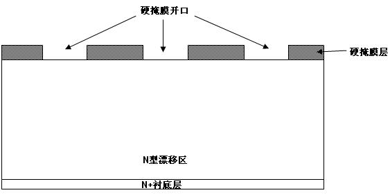
[0042] a. Provide a semiconductor substrate with N-type conductivity (the material includes silicon), the semiconductor substrate has a corresponding first main surface (the upper surface of the semiconductor substrate) and a second main surface (the lower surface of the semiconductor substrate), and the second main surface of the semiconductor substrate An N-type drift region and an N+ substrate layer are included between the first main surface and the second main surface, and the impurity concentration of the N+ substrate layer is greater than the impurity concentration of the N-type drift region; figure 1 shown.

[0043] b. Deposi...


PUM


Abstract

The invention discloses a manufacturing method for semiconductor devices with super junction structures. Second conductive type columns are achieved through a tilt angle implantation technology; the concentration, width and depth of the second conductive type columns can be more easily controlled by adjusting the implantation dose, the implantation energy and the implantation angle; and the width of the second conductive type columns can be greatly decreased; so that the width of whole P-N column pairs is reduced, simultaneously, the proportion of the width of first conductive type columns accounting for the width of P-N column pairs is increased, and the purpose of reducing on-resistance is reduced. First conductive type epitaxial layers are filled in deep grooves, and the first conductive type epitaxial layers and first conductive type mesa areas among the second conductive type columns form the first conductive type columns to improve the current flow path together when devices power on, accordingly, the flow path of current is increased greatly, and further the on-resistance is effectively reduced.

Description

technical field [0001] The invention relates to a method for manufacturing a semiconductor device, in particular to a method for manufacturing a semiconductor device with a super junction structure. Background technique [0002] In the field of medium and high voltage power semiconductor devices, the super junction structure (Super Junction) has been widely used. Compared with traditional power MOSFET devices, the super junction structure can obtain a better compromise relationship between device withstand voltage and on-resistance. The super junction structure is formed in the drift region of the device, which includes N-conductivity type columns (N-columns) and P-conductivity-type columns (P-columns), and multiple P-N column pairs formed by alternately adjoining N-columns and P-columns superjunction structure. The N column has impurities of N conductivity type, the P column has impurities of P conductivity type, and the impurity amount of the N column is consistent with t...

Claims


Application Information

Patent Timeline
Patent Type & Authority Applications(China)
IPC IPC(8): H01L21/336H01L21/265
Inventor 朱袁正李宗清叶鹏
Owner WUXI NCE POWER
Why Eureka
Try Eureka