Laser beam applying mechanism and laser processing apparatus

一种照射机构、激光束的技术,应用在激光器、激光焊接设备、激光器零部件等方向,能够解决降低半导体芯片质量、妨碍激光光线、难以确实地除去测试用金属图案区域等问题

Active Publication Date: 2012-08-08
DISCO CORP
View PDF11 Cites 10 Cited by
  • Summary
  • Abstract
  • Description
  • Claims
  • Application Information

AI Technical Summary

Problems solved by technology

Also, the Low-k film has the problem that since it is laminated in multiple layers (5 to 15 layers) like mica and is very brittle, when the Low-k film is cut along the dicing line by a cutting knife, the Low-k film is peeled off, and the peeled-off reaches the circuit. Semiconductor chips bring fatal damage
[0006] However, in a semiconductor wafer in which a test metal pattern called a test element group (TEG) for testing circuit functions is partially arranged on the Low-k film on the dicing line, there is a problem that even if the Low-k film is irradiated with laser light to remove the The metal pattern made of copper or aluminum hinders the laser light and cannot remove the Low-k film smoothly
In addition, when the output of the laser beam is increased to the extent that the metal pattern can be removed and the laser beam is irradiated to the scribe line, the following new problem also occurs: the semiconductor substrate only in the scribe line portion where the Low-k film is formed is broken and fragmented. Flying, the debris adheres to the bonding pads connected to the circuit, etc., deteriorating the quality of the semiconductor chip
[0010] However, it is difficult to adjust the output of the laser beam oscillated from the laser beam oscillator in accordance with the processing feed rate, and it is also difficult to reliably remove the area where the metal pattern for testing is located.

Method used


Image

  • Laser beam applying mechanism and laser processing apparatus
  • Laser beam applying mechanism and laser processing apparatus
  • Laser beam applying mechanism and laser processing apparatus

Examples


Embodiment Construction

[0049] Next, preferred embodiments of the laser beam irradiation mechanism and the laser processing apparatus according to the present invention will be described in detail with reference to the accompanying drawings.

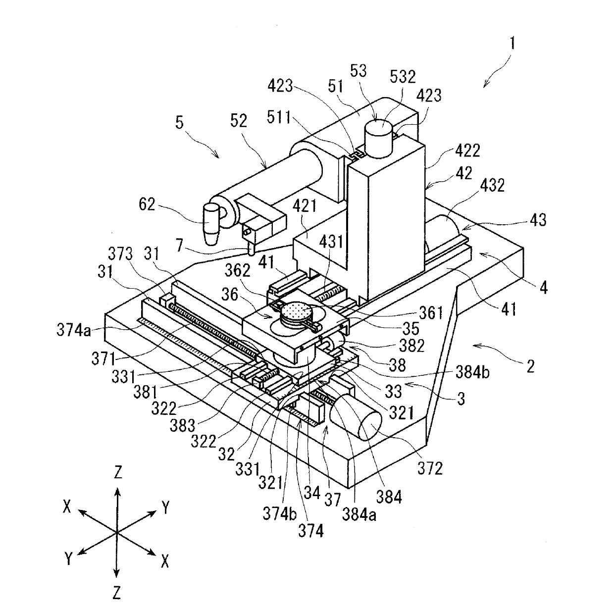
[0050] figure 1 It is a perspective view showing a laser processing apparatus equipped with a laser beam irradiation mechanism according to the present invention. figure 1 The illustrated laser processing apparatus 1 includes: a stationary base 2; a chuck table mechanism 3 arranged on the stationary base 2 so as to be movable in a machining feed direction (X-axis direction) indicated by an arrow X, Holding the workpiece; laser beam irradiation unit support mechanism 4, which is arranged on the stationary base so as to be movable in the index feed direction (Y-axis direction) indicated by arrow Y perpendicular to the X-axis direction 2; and a laser beam irradiation unit 5 disposed on the laser beam irradiation unit support mechanism 4 so as to be movable in a f...


PUM


Abstract

A laser beam applying mechanism has a power adjusting unit provided between a laser beam oscillator and a focusing lens. The power adjusting unit includes a half-wave plate, a prism having a first polarization beam splitter film and a second polarization beam splitter film. The optical path is adjusted by a piezoelectric actuator opposed to the first polarization beam splitter film, and a polarized light components synthesizer opposed to the second polarization beam splitter film generates a phase difference ([beta]) between an S polarized light component and a P polarized light component. The phase difference ([alpha+beta]) between the S polarized light component and the P polarized light component of the laser beam obtained by the polarized light components synthesizer is in the range of 0 DEG to 180 DEG .

Description

technical field [0001] The present invention relates to a laser beam irradiation mechanism and a laser processing device capable of high-speed control of the output of laser beam oscillated from a laser beam oscillator. Background technique [0002] In the manufacturing process of semiconductor devices, a plurality of regions are divided on the surface of a roughly disc-shaped semiconductor wafer by dividing lines called dicing lines arranged in a grid pattern, and devices such as ICs and LSIs are formed in the divided regions. . Then, the semiconductor wafer is cut along the dicing lines to divide the regions where the devices are formed to manufacture individual semiconductor devices. [0003] Severing of semiconductor wafers along dicing streets is usually performed by a cutting device called a dicing saw. This cutting device has: a chuck table, which holds a semiconductor wafer as a workpiece; a cutting unit, which cuts the semiconductor wafer held by the chuck table; ...

Claims


Application Information

Patent Timeline
Patent Type & Authority Applications(China)
IPC IPC(8): B23K26/36B23K26/42B23K26/08B23K26/06B23K26/00G02B26/06G02B27/28H01S3/00
CPCB23K26/0626B23K26/4075B23K26/064B23K26/40B23K2103/50B23K26/0643B23K26/0652B23K26/067
Inventor 能丸圭司
Owner DISCO CORP
Why Eureka
Try Eureka