Forming method for memory cell of flash memory

A technology of storage unit and flash memory, which is applied in the fields of electrical components, semiconductor/solid-state device manufacturing, circuits, etc. It can solve the problems of unfavorable development needs of flash memory miniaturization, insignificant performance improvement of flash memory, and large storage unit size, etc., to achieve programming Effects related to improved reading efficiency, reduced size, and improved retention

Active Publication Date: 2012-08-15
SHANGHAI HUAHONG GRACE SEMICON MFG CORP
View PDF5 Cites 6 Cited by
  • Summary
  • Abstract
  • Description
  • Claims
  • Application Information

AI Technical Summary

Problems solved by technology

[0006] However, the efficiency of covering the stress layer on the surface of the control gate layer 14 and the source line layer 11 on the carrier mobility in the channel region is not high, and the data retention is low, resulting in insignificant improvement in the performance of the flash memory; moreover, covering The stress layer will increase the size of the storage unit of the flash memory, which is not conducive to the development of the miniaturization of the flash memory

Method used


Image

  • Forming method for memory cell of flash memory
  • Forming method for memory cell of flash memory
  • Forming method for memory cell of flash memory

Examples


Embodiment Construction

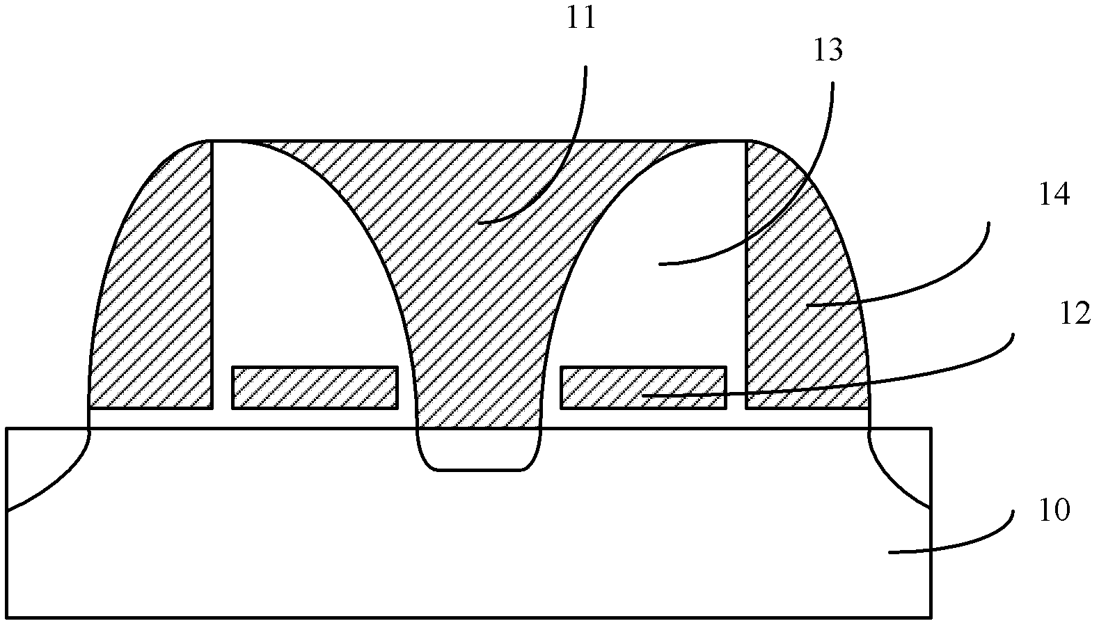
[0043] As described in the background technology, the memory cell of the flash memory covered with the stress layer in the prior art does not greatly improve the carrier mobility, and the data retention is low, resulting in little improvement in the performance of the flash memory; moreover, the stress layer covered will Enlarging the size of the storage unit of the flash memory is not conducive to the miniaturization development requirements of the flash memory.

[0044] The inventors of the present invention have found through research that the increase in carrier mobility is not so great because the stress provided by the stress layer can only be conducted to the channel region of the semiconductor substrate through the source line layer and the control gate layer, so The stress conducted into the channel region is small, and the carrier mobility is not greatly improved; and the covered stress layer will occupy space, making the size of the memory cell of the flash memory la...


PUM

PropertyMeasurementUnit
thicknessaaaaaaaaaa

Abstract

The invention discloses a forming method for a memory cell of a flash memory. The forming method comprises the steps of: providing a semiconductor substrate; forming a first insulating layer on the surface of the semiconductor substrate; forming a floating gate polycrystalline silicon layer on the surface of the first insulating layer; forming a stress layer on the surface of the floating gate polycrystalline silicon layer; after the forming of the stress layer, conducting thermal annealing on the stress layer, the floating gate polycrystalline silicon layer, the first insulating layer and the semiconductor substrate; after thermal annealing, removing the stress layer; after the removal of the stress layer, forming a source line layer passing through the floating gate polycrystalline silicon layer and the first insulating layer on the surface of the semiconductor substrate; and removing part of the floating gate polycrystalline silicon layer and forming a floating gate layer on the surface of the first insulating layer on two sides of the source line layer, wherein the floating gate layer is electrically isolated from the source line layer. The forming method for the memory cell of the flash memory can retain stress inside the floating gate layer, thereby enhancing the channel carrier mobility of the memory cell of the flash memory and reducing the size of the memory cell of the flash memory simultaneously when improving the data retention.

Description

technical field [0001] The invention relates to the field of semiconductor manufacturing, in particular to a method for forming a storage unit of a flash memory. Background technique [0002] In the current semiconductor industry, integrated circuit products can be mainly divided into three types: analog circuits, digital circuits and digital / analog hybrid circuits, among which storage devices are an important type of digital circuits. In recent years, among storage devices, flash memory (flash memory) has developed particularly rapidly. The main feature of flash memory is that it can keep stored information for a long time without power on; and it has the advantages of high integration, fast access speed, easy erasing and rewriting, etc., so it has been widely used in many fields such as microcomputer and automatic control. a wide range of applications. [0003] In the prior art, please refer to the storage unit of the flash memory figure 1 ,include: [0004] A semicond...

Claims


Application Information

Patent Timeline
Patent Type & Authority Applications(China)
IPC IPC(8): H01L21/8247
Inventor 于涛胡勇李冰寒
Owner SHANGHAI HUAHONG GRACE SEMICON MFG CORP
Why Eureka
Try Eureka