White-light emitting diode with vertical structure and manufacturing method thereof

A technology of light-emitting diodes and vertical structures, applied in electrical components, circuits, semiconductor devices, etc., can solve the problems of complex production process of vertical structure LEDs, reduce product stability and yield, and increase production costs, and achieves the advantages of separating, The effect of ensuring stability and reducing the difficulty of cutting

Inactive Publication Date: 2012-08-15
TONGFANG OPTO ELECTRONICS
View PDF5 Cites 11 Cited by
  • Summary
  • Abstract
  • Description
  • Claims
  • Application Information

AI Technical Summary

Problems solved by technology

The disadvantage of this method is that the driving circuit of the LED is more complicated and the cost is higher.
However, the production process of vertical structure LEDs is relatively complicated, which will reduce the stability and good rate of products, and greatly increase production costs

Method used


Image

  • White-light emitting diode with vertical structure and manufacturing method thereof
  • White-light emitting diode with vertical structure and manufacturing method thereof
  • White-light emitting diode with vertical structure and manufacturing method thereof

Examples


Embodiment Construction

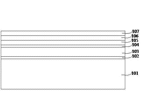
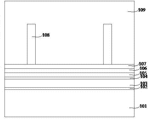
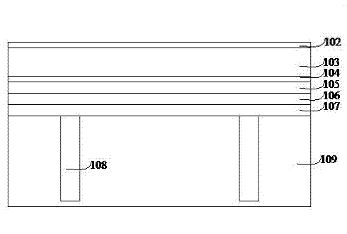
[0031] see Figure 10 The white light vertical light emitting diode of the present invention comprises a metal support substrate 109, a metal seed layer 107, a reflective metal layer 106, a P-type GaN-based semiconductor layer 105, a quantum well active region 104, and an N-type GaN-based semiconductor layer stacked sequentially from bottom to top. The semiconductor layer 103 and the passivation layer 110, a phosphor layer 111 is placed on the passivation layer 110, and an N-face electrode 112 is placed in the electrode groove at the top of the device. The metal supporting substrate 109 is made of Ni, Cu, Au, Fe, Mn, Sn or an alloy of several elements, and the thickness of the metal supporting substrate 109 is 100-500 μm. The material of the metal seed layer 107 is composed of one or more layers of metals among Pd, Pt, Au, W, Ni, Ta, Co, Ru, and the thickness of the metal seed layer 107 is 100-400 nm. The reflective metal layer 106 is made of Al or Ag and their alloys with h...


PUM

PropertyMeasurementUnit
thicknessaaaaaaaaaa
thicknessaaaaaaaaaa

Abstract

The invention discloses a white-light emitting diode with a vertical structure and a manufacturing method thereof and relates to the fields of illumination and manufacturing of semiconductor photoelectric devices and semiconductors. The white-light emitting diode disclosed by the invention comprises a metal supporting substrate, a metal seed layer, a reflecting metal layer, a P-type GaN-based semiconductor layer, a quantum well source region, an N-type GaN-based semiconductor layer and a passivation layer which are sequentially superposed form bottom to top, wherein an electrode trough on the top of a device is provided with an N-face electrode. The white-light emitting diode is structurally characterized in that a fluorescent powder layer is arranged on the passivation layer. Compared with the prior art, the white-light emitting diode disclosed by the invention is capable of effectively improving the luminescence power of the device and has the characteristics of simple process and low cost.

Description

technical field [0001] The invention relates to the fields of semiconductor optoelectronic devices and semiconductor lighting manufacturing, in particular to a GaN-based vertical structure white light emitting diode and a manufacturing method thereof. Background technique [0002] In recent years, GaN-based white LEDs, as a new type of energy-saving and environmentally friendly light source, have become a hot issue in the field of solid-state lighting research. White light LED has the characteristics of miniaturization, long life, planarization, and strong designability, etc., and can realize large-scale planar lattice; at the same time, white light LED does not contain lead and mercury that are harmful to human body, avoiding environmental pollution; moreover, white light LED LED has no strobe, pure light chromaticity, the radiation area is mainly concentrated in the visible light area, and hardly generates heat, so it is energy-saving and environmentally friendly, and can...

Claims


Application Information

Patent Timeline
Patent Type & Authority Applications(China)
IPC IPC(8): H01L33/00
Inventor 徐亮刘刚郭德博张华东
Owner TONGFANG OPTO ELECTRONICS
Why Eureka
Try Eureka