Method for uninterrupted growth of high-quality InGaN/GaN multi-quantum well (MQW)

A multi-quantum well, high-quality technology, applied in the field of quantum well growth, can solve the problems of low time utilization rate and intermittent growth of quantum wells, and achieve the effect of shortening time and improving production efficiency

Active Publication Date: 2012-08-15
INST OF SEMICONDUCTORS - CHINESE ACAD OF SCI
View PDF3 Cites 24 Cited by
  • Summary
  • Abstract
  • Description
  • Claims
  • Application Information

AI Technical Summary

Problems solved by technology

Due to the differences in the growth temperature and atmosphere between InGaN quantum wells and GaN quantum barriers, there is a lot of time spent in switching the temperature and atmosphere required for the growth of quantum wells and

Method used


Image

  • Method for uninterrupted growth of high-quality InGaN/GaN multi-quantum well (MQW)
  • Method for uninterrupted growth of high-quality InGaN/GaN multi-quantum well (MQW)
  • Method for uninterrupted growth of high-quality InGaN/GaN multi-quantum well (MQW)

Examples


Embodiment

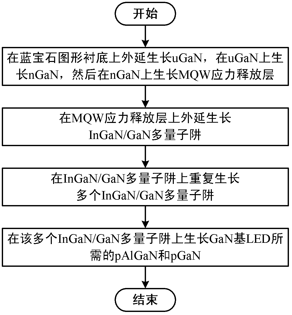
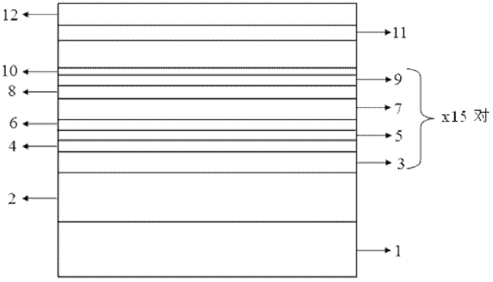
[0047] Utilize MOCVD equipment (Crius 31 commercial machine of Aixtron Company), select high-purity NH 3 As N source, high-purity N 2 and H 2 As carrier gas, trimethylindium (TMIn) and trimethylaluminum (TMAl) are used as indium source and aluminum source respectively, trimethylgallium (TMGa) is used as gallium source of GaN material, and triethylgallium (TEGa) is used as InGaN Ga source for GaN multiple quantum wells, silane (SiH 4 ) is an N-type dopant, and dicene Mg (Cp2Mg) is a P-type dopant. Epitaxially grow uGaN1 on the sapphire pattern substrate, then grow nGaN2 on uGaN1, and then grow MQW stress release layer 3 on nGaN2, the MQW stress release layer 3 adopts InGaN / GaN superlattice structure SLs, SLs logarithm is 4, the growth temperature is 900°C, and the thickness of InGaN in the InGaN / GaN superlattice structure SLs is The thickness of GaN is

[0048] Choose high-purity N 2 As the carrier gas, the InGaN quantum well 4 is epitaxially grown on the MQW stress re...


PUM


Abstract

The invention discloses a method for uninterrupted growth of a high-quality InGaN/GaN multi-quantum well (MQW). The method comprises the following steps of: carrying out uGaN epitaxial growth on a sapphire-patterned substrate, growing nGaN on uGaN, and then, growing an MQW stress release layer on nGaN; carrying out InGaN/GaN MQW epitaxial growth on the MQW stress release layer; repeatedly growing a plurality of InGaN/GaN MQWs on the InGaN/GaN MQW; and growing pAlGaN and pGaN needed by a GaN-based LED (Light Emitting Diode) on the InGaN/GaN MQWs. According to the method for the uninterrupted growth of the high-quality InGaN/GaN MQW, a metal organic chemical vapor deposition method is adopted, and the growth of the GaN is kept during the process of switching growing conditions for quantum wells and quantum barriers, namely the uninterrupted growth of the quantum wells, so that the time required for the growth of the MQW is shortened, the production efficiency is greatly increased, and meanwhile, an LED epitaxial wafer with the high-quality InGaN/GaN MQW is obtained.

Description

technical field [0001] The invention relates to the technical field of quantum well growth, in particular to a method for growing high-quality InGaN / GaN multiple quantum wells without interruption, which is suitable for commercial production of high-brightness GaN-based LED epitaxial wafers. Background technique [0002] GaN-based LEDs have now entered the stage of commercial production. How to shorten the growth time of GaN-based LED epitaxial wafers while obtaining high-quality epitaxial wafers to increase production capacity has become a research focus. At present, MOCVD is used for commercial production of GaN-based LED epitaxial wafers. Due to the differences in the growth temperature and atmosphere between InGaN quantum wells and GaN quantum barriers, there is a lot of time spent in switching the temperature and atmosphere required for the growth of quantum wells and quantum barriers during the growth of InGaN / GaN multiple quantum wells. Quality generally does not und...

Claims


Application Information

Patent Timeline
IPC IPC(8): H01L33/00H01L21/20
Inventor 李盼盼李鸿渐张逸韵李志聪梁萌李璟王国宏
Owner INST OF SEMICONDUCTORS - CHINESE ACAD OF SCI
Why Eureka
Try Eureka