Micromechanical method and corresponding assembly for bonding semiconductor substrates and correspondingly bonded semiconductor chip

A substrate bonding and semiconductor technology, applied in semiconductor devices, microstructure devices, processing microstructure devices, etc., can solve problems such as liquid eutectic phase inflow

Inactive Publication Date: 2012-09-12
ROBERT BOSCH GMBH
View PDF5 Cites 6 Cited by
  • Summary
  • Abstract
  • Description
  • Claims
  • Application Information

AI Technical Summary

Problems solved by technology

This leads to the extension of the liquid eutectic phase
At this time, it may appear that the liquid eutectic phase flows into the MEMS functional area uncontrollably

Method used


Image

  • Micromechanical method and corresponding assembly for bonding semiconductor substrates and correspondingly bonded semiconductor chip
  • Micromechanical method and corresponding assembly for bonding semiconductor substrates and correspondingly bonded semiconductor chip
  • Micromechanical method and corresponding assembly for bonding semiconductor substrates and correspondingly bonded semiconductor chip

Examples


Embodiment Construction

[0024] In the figures, the same reference symbols designate the same or functionally identical components.

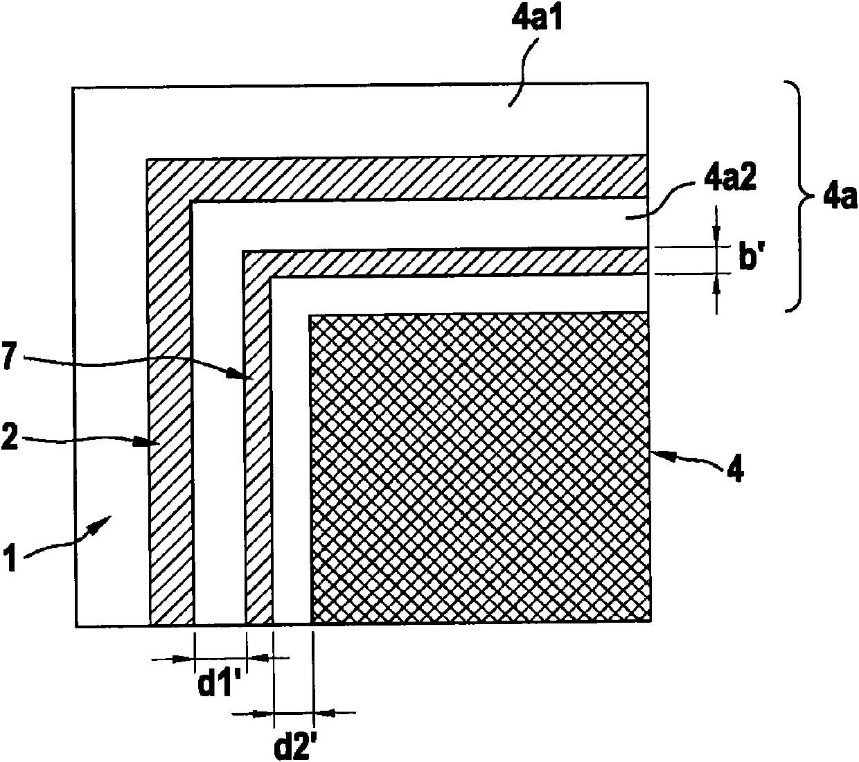
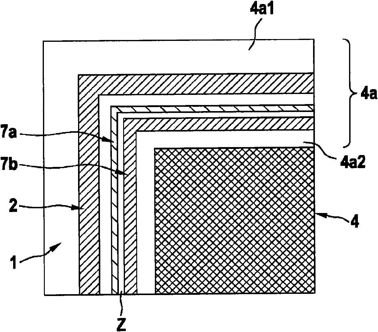
[0025] Figure 1a is a schematic partial top view of the chip region of the semiconductor substrate bonding device according to the first embodiment of the present invention.

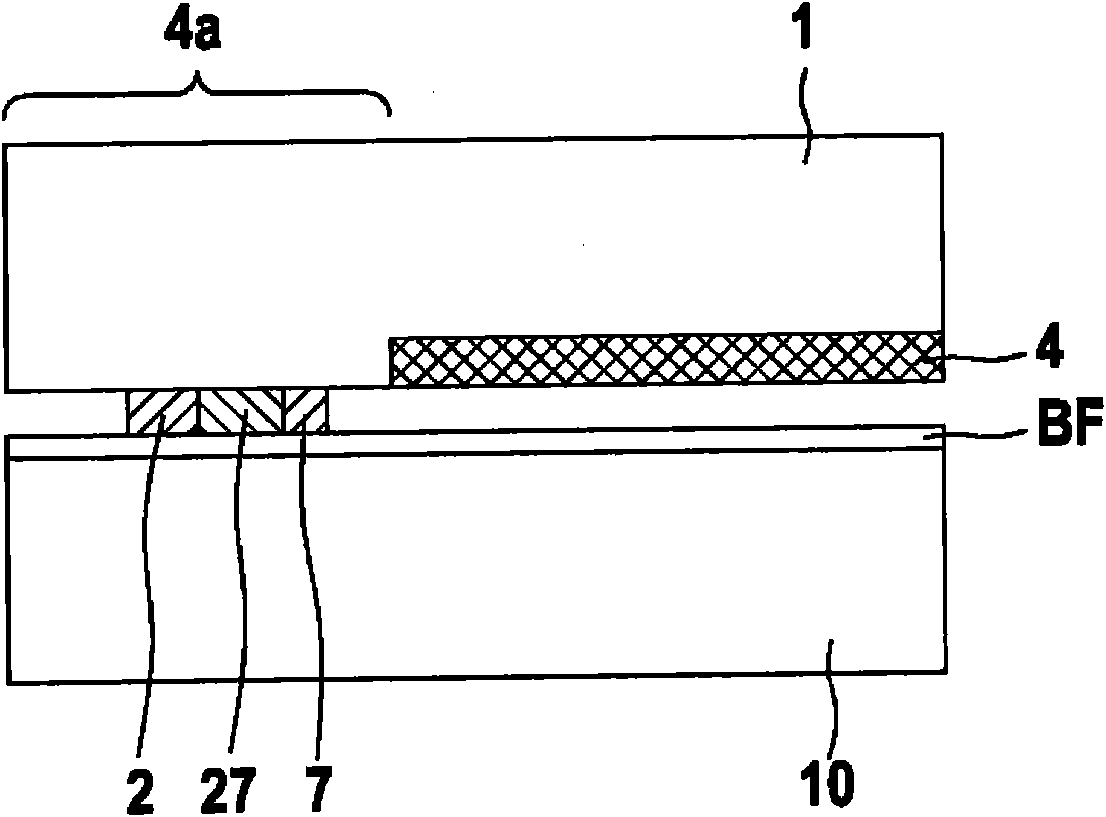
[0026] The micromechanical sensor chip 1 has an active functional region 4 and an inactive edge region 4 a. In the edge region 4a is arranged a joint frame 2 with applied thereto a eutectic bonding alloy such as Al-Ge, which divides the edge region 4a into an inner region 4a2 surrounded by the bond frame and an outer region 4a1. In the inner region 4a2 between the junction frame 2 and the functional area 4 of the sensor chip 1 is provided a flow stop frame 7 which is formed of a non-eutectic alloy of Al and Ge and thus has a Ge content, or higher than the Al content of the corresponding eutectic alloy (up to the respective pure alloy composition).

[0027] When the attached flow stop frame 7 i...


PUM


Abstract

The invention relates to a micromechanical method and a corresponding assembly for bonding semiconductor substrates and a correspondingly bonded semiconductor chip. The assembly according to the invention comprises a semiconductor substrate having a chip pattern having a plurality of semiconductor chips (1), each having a functional region (4) and an edge region (4a) surrounding the functional region (4), wherein there is a bonding frame (2) made of a bonding alloy made from at least two alloy components in the edge region (4a), spaced apart from the functional region (4). Within the part (4a2) of the edge region (4a) surrounding the bonding frame (2) between the bonding frame (2) and the functional region (4), there is at least one stop frame (7; 7a, 7b; 7b'; 70) made of at least one of the alloy components, which is designed such that when a melt of the bond alloy contacts the stop frame (7; 7a, 7b; 7b'; 70) during bonding, the bonding alloy solidifies.

Description

technical field [0001] The invention relates to a micromechanical method for bonding semiconductor substrates and a corresponding device as well as a corresponding bonded semiconductor chip. Background technique [0002] Although the invention can be applied to any micromechanical components and structures, in particular sensors and actuators, the problem with the invention and the micromechanical sensors on which it is based can be produced with silicon surface micromechanics is also explained. [0003] Micromechanical substrate bonding, eg wafer-wafer-bonding-bonding, is typically achieved using eutectic alloys or alloy components with two or more solid bonding materials as components. Such eutectic alloys have a uniquely definable melting point. Conversely, other mixing ratios of the same alloy components have melting or solidifying regions in which solid phases are present in addition to the melt. In addition, eutectic alloys have the lowest melting point of all mixtur...

Claims


Application Information

Patent Timeline
Patent Type & Authority Applications(China)
IPC IPC(8): B81C3/00
CPCB81C1/00269B81C2201/019B81C2203/0118B81C2203/019B81C2203/036H01L23/10H01L24/29H01L24/30H01L24/32H01L24/83H01L25/50H01L2224/26145H01L2224/29011H01L2224/29013H01L2224/29076H01L2224/291H01L2224/29117H01L2224/29124H01L2224/30051H01L2224/30131H01L2224/30135H01L2224/30177H01L2224/30505H01L2224/30515H01L2224/32054H01L2224/32145H01L2224/32501H01L2224/83007H01L2224/83095H01L2224/83191H01L2224/83365H01L2224/83815H01L2924/01013H01L2924/01029H01L2924/01032H01L2924/0105H01L2924/01079H01L2924/01082H01L2924/1631H01L2924/165H01L2924/01005H01L2924/01006H01L2924/01033H01L2924/01322H01L2924/014H01L2224/29101H01L2924/0132H01L2224/29111H01L2224/29109H01L2224/29144H01L2924/1461H01L2924/00H01L2924/01014H01L2924/01049H01L2924/00014
Inventor A·特劳特曼R·赖兴巴赫
Owner ROBERT BOSCH GMBH
Why Eureka
Try Eureka